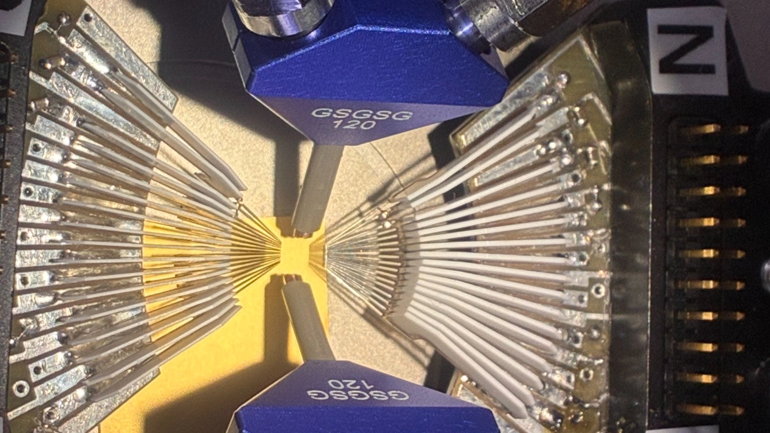
Advanced packaging is changing more than the physical structure of semiconductor devices. It is also changing where engineers need to access, characterize and validate high-speed electrical signals.
As architectures move toward chiplets, heterogeneous integration and denser package structures, more of the critical electrical path is moving closer to the silicon. A signal that once could be treated mainly as a board-level problem may now pass through redistribution structures, bumps, interposers, package substrates and localized electrical access structures before it reaches the PCB.
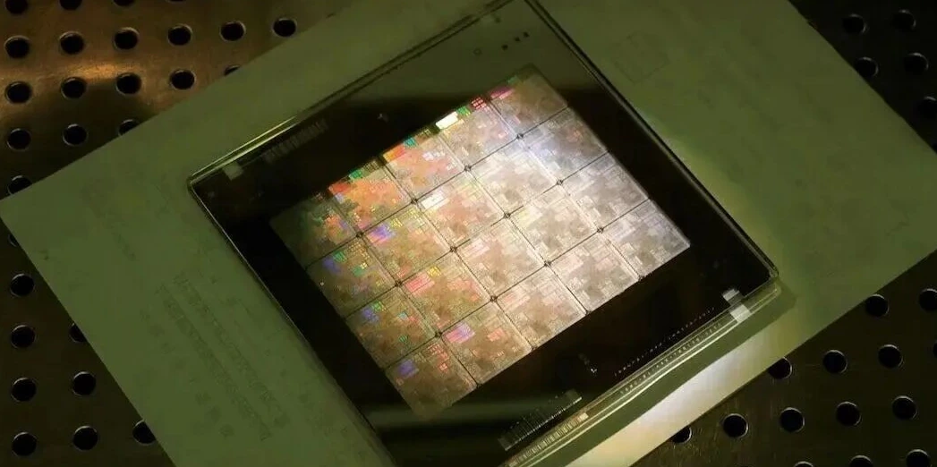
The probe architecture should be determined by the measurement plane and DUT geometry — not only by frequency range.
From a measurement perspective, the key question is not simply whether the instrument and probe support enough bandwidth. It is:
How can engineers obtain controlled electrical access to the structure being measured without allowing the measurement interface itself to dominate the result?
From PCB-Level Testing to Advanced Package Characterization
Traditional PCB-level RF testing often provides relatively accessible measurement locations: connectors, transmission-line structures, evaluation boards and dedicated test coupons.
Advanced packaging introduces a different access problem. The electrical path may become physically smaller, mechanically less accessible and electrically more complex while the required measurement uncertainty becomes more demanding.
The measurement target may move from a board-level launch toward:
- fine-pitch die pads,
- package transitions,
- interposer or substrate structures,
- localized test access close to the die.
The challenge therefore shifts from “How do we connect to the board?” toward “How do we access the electrical behavior inside a much smaller and more complex structure?”
At microwave and mmWave frequencies, the probe transition, contact geometry, fixture structure, cable behavior, calibration reference plane and local DUT access can all influence the measured response. Advanced-package characterization therefore requires a complete measurement-path view rather than a probe-only view.
The Measurement Plane Determines the Probe Requirement
One of the most important decisions in RF probing is defining the intended measurement plane. The same system can require very different probing priorities depending on where the electrical behavior needs to be observed.
| Measurement Plane | Typical Structure | Primary Probe Challenge |
|---|---|---|
| Wafer / die | Fine pads and localized electrical structures | Small contact geometry, fine pitch and precise positioning |
| Package / test structure | Interposer, substrate and package transitions | Localized access and controlled transition characterization |
| PCB / PCBA | Evaluation boards and system test structures | Mechanical robustness, clearance and repeatable contact |
These measurement environments are not interchangeable. A probe optimized for repeated PCB validation should not automatically be assumed suitable for fine-pitch die-level access, and a precision wafer probe is not automatically the most practical architecture for repeated board-level measurements.
A useful selection sequence is:
Wafer-Level RF Probing: Accessing Fine-Pitch Structures
As the measurement plane moves closer to the die, physical access becomes a first-order engineering constraint.
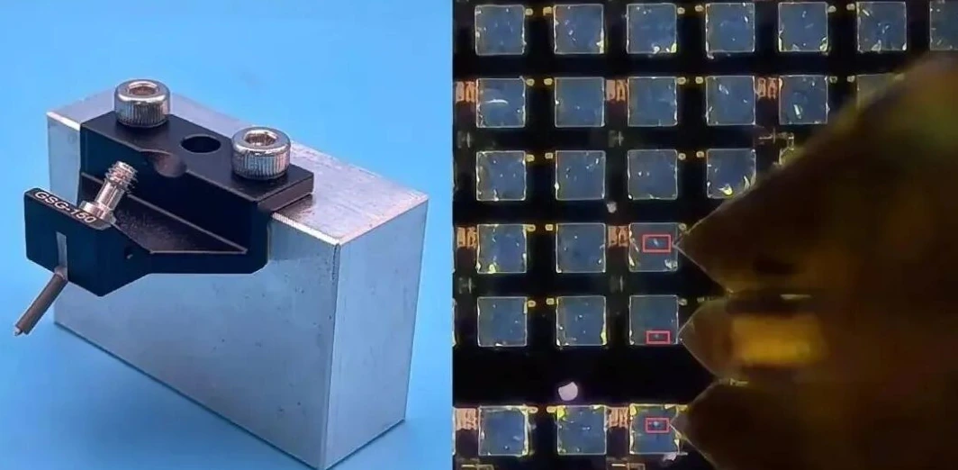
Wafer- and die-level structures can involve smaller pads, tighter pitch, limited landing area and higher positioning sensitivity. At this scale, the probe is not simply a connection point; it is a precision interface between the measurement system and a small electrical structure.
Three factors become especially important:
- Contact geometry: the probe contact must be appropriate for the available pad structure.
- Positioning accuracy: smaller landing areas make alignment directly relevant to repeatability.
- Repeatable contact: the measurement requires controlled behavior across repeated touchdowns, not merely electrical contact once.
For this type of precision access, the
AQUILA™ precision RF probe platform
is positioned around microwave/mmWave wafer characterization and fine-pad measurement requirements.
The important point is not that a particular probe series is universally “for advanced packaging.” It is that precision access becomes more important as the measurement plane moves closer to the die.
Package-Level RF Characterization: Measuring Through Complex Transitions
At package level, the package itself becomes part of the electrical channel.
Depending on the architecture, the measured path may include redistribution layers, bumps, vias, interposers, substrate routing and transitions between different transmission structures. These are not electrically invisible connections.
The relevant question is therefore not only whether a signal can pass through the package, but how the complete electrical path behaves over the required frequency range.
Potential contributors to the measured response include:
- impedance variation,
- via and substrate transitions,
- return-path changes,
- asymmetry in differential structures,
- probe and access-transition discontinuities.
This is why package-level characterization needs a clearly defined measurement reference plane. A measurement taken at a package access point does not automatically represent the electrical behavior at an internal die-to-die interface; the structures between those locations remain part of the measured network unless they are separately characterized and, where appropriate, removed mathematically.
Localized Electrical Access
Package-level test structures may not provide the large, convenient access points found on a PCB. Engineers may need to land on small exposed pads, dedicated test vehicles or localized characterization structures.
The measurement interface therefore has to balance two requirements: provide reliable physical access while adding as little uncontrolled electrical disturbance as practical.
PCB-Level Validation After Advanced Packaging
Advanced packaging does not eliminate PCB-level validation. Once signals leave the package, they still travel through package breakouts, PCB traces, connectors, modules, cables and other system-level interfaces.
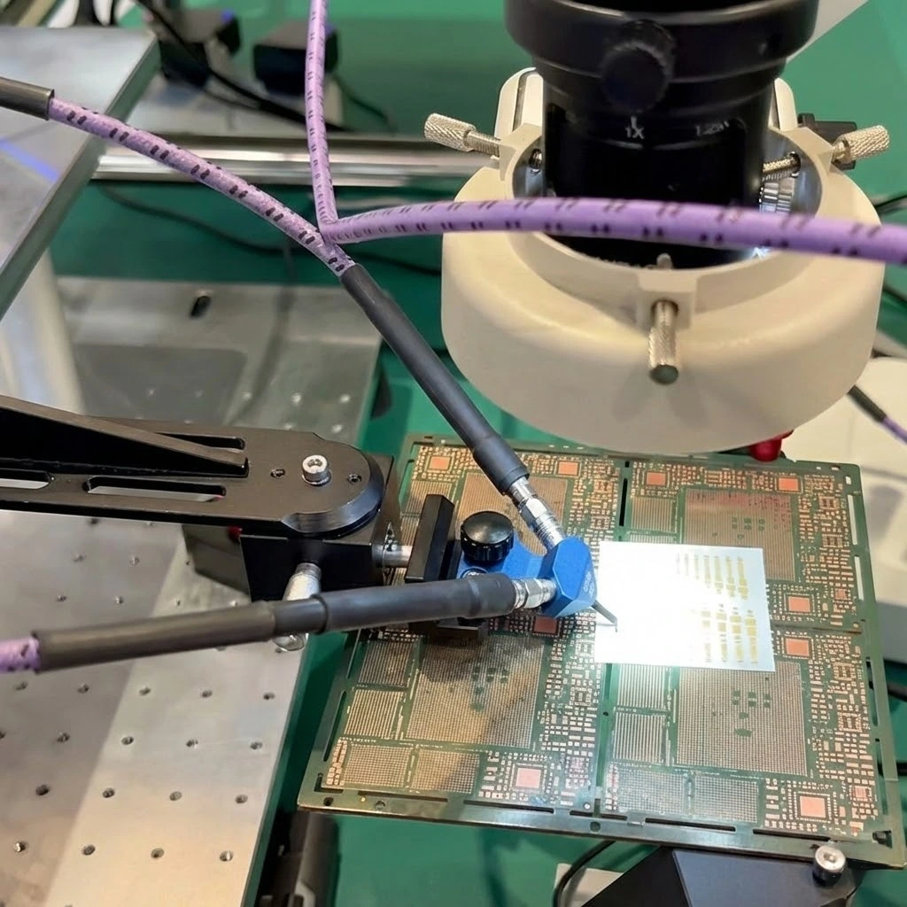
Board-level measurement therefore remains essential for evaluating the complete channel under realistic engineering conditions.
The optimization priorities, however, are different from fine-pitch wafer probing. PCB environments often place greater emphasis on:
- mechanical robustness,
- repeatable contact,
- practical mechanical access,
- stable behavior over repeated test cycles.
For PCB and repeated-test environments, the
LYRA™ ACP RF probe platform
emphasizes robust board-level probing and high-touchdown measurement requirements.
Why Frequency Rating Alone Is Not Enough
Frequency range is important, but it should not be treated as the only probe-selection criterion.
A higher-frequency probe is not automatically the correct probe for every measurement task.
A practical RF measurement depends on the interaction between:
- required bandwidth,
- DUT geometry,
- pitch and contact topology,
- landing area and mechanical clearance,
- cable and interface performance,
- calibration strategy,
- desired measurement reference plane.
A fine-pitch die structure may require a precision contact architecture even when the intended measurement does not use the highest available probe bandwidth. Conversely, a PCB validation task may benefit more from a mechanically robust probe architecture and repeatable landing than from selecting the highest-frequency probe available.
This leads to a more useful rule:
Calibration and Reference Plane Considerations
An RF probe does not measure the DUT in isolation. The complete measurement path may include:
Each element can contribute loss, reflection or transition behavior to the measured response. The engineer therefore needs to understand which part of the result belongs to the DUT and which part belongs to the measurement environment.
Calibration establishes a corrected reference plane according to the selected calibration method. When the desired electrical reference plane lies deeper inside a package, access structure or fixture, additional characterization and de-embedding may be required.
De-embedding does not replace calibration. The two operations address different parts of the measurement path.
The closer the desired reference plane moves toward the structure of interest, the more important fixture characterization and access-transition control become.
The instrument-side interconnect also matters.
RF coaxial cables and test interconnects
need to support the required bandwidth while maintaining stable routing and connection repeatability.
The broader
Vinstronics RF probe platform
covers different wafer- and PCB-oriented probing architectures; the appropriate configuration depends on measurement plane, DUT geometry, contact topology and bandwidth requirements.
Advanced Packaging in AI and High-Speed Computing Systems
AI and high-performance computing are increasing the demand for higher bandwidth density and tighter integration. More data has to move through increasingly complex electrical paths that can span die-level interconnects, package transitions, PCB channels and the electrical side of high-speed optical interfaces.
That makes advanced-package characterization a natural extension of the broader high-speed measurement problem discussed in
RF Probing for AI Accelerators, Chiplets and High-Speed Computing: What Engineers Actually Measure
.
The application changes, but the measurement fundamentals remain consistent:
- Where is the electrical path?
- Where should the reference plane be established?
- How can the DUT be accessed?
- How much does the measurement interface influence the result?
RF probing is one part of that characterization chain. The probe provides access; the instrument, interconnect, calibration and DUT structure together determine the usable measurement.
Conclusion
Advanced packaging is changing the physical location and mechanical scale of high-frequency electrical measurement.
For wafer and fine-pitch structures, precision access and positioning become critical. For package-level characterization, transitions and reference-plane definition become central. For PCB-level validation, robustness and repeatability remain important.
The correct RF probe is therefore not defined by frequency range alone.
FAQ
What is RF probing used for in advanced packaging?
RF probing provides controlled electrical access to structures that may not have conventional RF connectors. It can support characterization of loss, reflections, impedance behavior and transitions across wafer, package and PCB measurement environments.
Why does advanced packaging require different probing strategies?
Because wafer, package and PCB measurement planes present different pad geometries, pitches, access constraints, mechanical environments and reference-plane requirements. The same probe architecture should not be assumed suitable at every level.
Is a higher-frequency RF probe always better?
No. Frequency capability is only one selection factor. DUT geometry, pitch, contact topology, mechanical access, calibration and measurement plane are also critical.
What is the difference between wafer-level and PCB-level RF probing?
Wafer-level probing typically emphasizes fine contact geometry, small landing areas and precise positioning. PCB-level probing often places greater emphasis on mechanical robustness, clearance and repeatable contact across multiple measurements.
How does measurement plane affect probe selection?
The measurement plane determines the physical access problem and the electrical transition presented to the probe. Probe architecture should therefore be matched to the DUT geometry and intended reference plane before bandwidth is considered in isolation.
Need to Define the Right RF Probe Architecture?
Send the DUT type, measurement plane, landing geometry and required bandwidth. Vinstronics can review the appropriate probe and RF interconnect approach for your test setup.