
Precision Solderless PCB Connectors
Compression-mounted RF transitions for PCB validation, fixture interfaces and microwave / millimeter-wave board characterization up to 110 GHz.

Start with the launch path
Selection starts with the physical launch path: vertical Z-axis access from the board surface, or end launch from the PCB edge.

Vertical Launch
Used when the RF transition must enter the PCB from the top surface for center-of-board, dense test area or multilayer board access.
- Best for Z-axis access and internal signal locations.
- Typical for ATE boards, dense RF layouts and mmWave validation fixtures.
- Confirm PCB thickness, signal layer, ground reference and mounting area.

End Launch
Used when the RF path exits through the PCB edge and a collinear board-edge transition is required for high-speed evaluation.
- Best for board-edge and straight-line RF transitions.
- Typical for SerDes channels, optical module boards and RF test fixtures.
- Confirm board-edge geometry, pad dimensions, via fence and available height.
Featured solderless connector types
Representative products selected to show launch path, frequency ceiling and interface coverage. Full model browsing remains available through the solderless PCB connector archive.
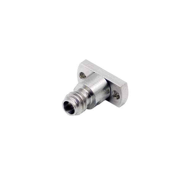
1.0mm Vertical Solderless PCB Connector
Flagship vertical launch option for ultra-high-frequency PCB validation and mmWave / sub-THz test structures.
- DC–110 GHz 1.0mm female interface.
- Two-hole solderless mount for repeatable board installation.
- Designed for straight PCB launch and compact fixtures.
- PCB layout and signal pad should be confirmed by drawing.

1.0mm Low-Profile End Launch Connector
Board-edge end launch structure for height-sensitive layouts requiring controlled 110 GHz transition performance.
- DC–110 GHz 1.0mm female end launch interface.
- Low-profile format for compact board-edge integration.
- Suitable for mmWave test fixtures and precision assemblies.
- Board edge geometry and via pattern require drawing review.
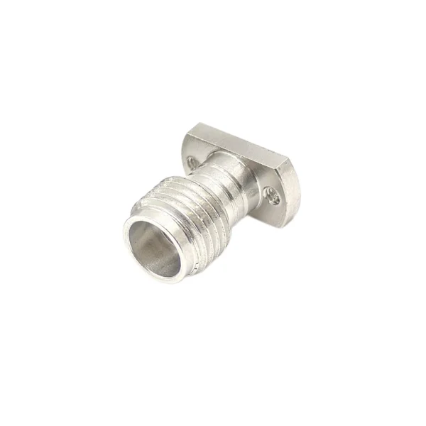
1.85mm Vertical Solderless PCB Connector
High-frequency Z-axis PCB launch for 67 GHz evaluation boards where repeatability and low discontinuity matter.
- DC–67 GHz 1.85mm jack interface.
- Two-hole flange for stable board attachment.
- Used for compact 1.85mm test boards and fixtures.
- Ground ring and signal pad geometry should be reviewed.
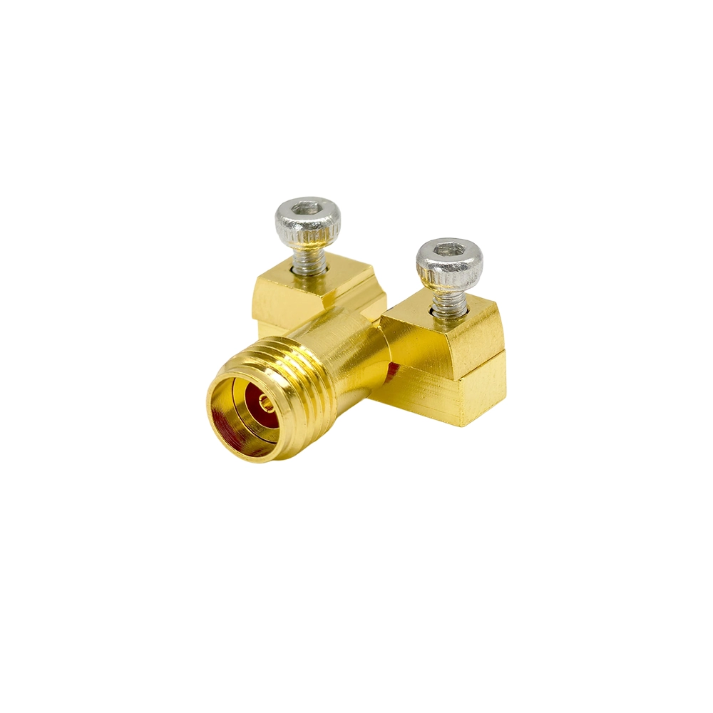
2.92mm End Launch PCB Connector
Mainstream K connector board-edge launch for 40 GHz microwave boards, fixtures and compact assemblies.
- DC–40 GHz 2.92mm female end launch structure.
- Compact right-angle format for PCB edge integration.
- Suitable for microwave test fixtures and RF assemblies.
- PCB thickness and recommended signal pad confirmed by drawing.
Browse the full solderless PCB connector archive, including vertical launch, end launch, 1.0mm, 1.85mm, 2.4mm, 2.92mm and SMA options.
View all solderless PCB products →What solderless solves
Solderless connectors reduce assembly variation, avoid heat exposure on expensive RF substrates and support reusable connectorized access across multiple prototype boards.
Key benefits
- No solder reflow on Rogers, Megtron and other RF substrates.
- Reusable test interface for multiple board iterations.
- Torque-controlled mounting for repeatable contact pressure.
- Vertical and end launch options for board-level RF access.
- Interface families from SMA and 2.92mm up to 1.0mm configurations.
Typical applications
- Semiconductor validation boards and ATE load boards.
- 112G / 224G SerDes and 800G / 1.6T networking validation.
- RF and mmWave instrumentation fixtures.
- Optical module test boards and high-speed evaluation platforms.
- Microwave prototypes where connector rework must be minimized.
Selection reference
These solderless RF connectors are selected by interface family, launch direction, PCB stack-up and target frequency. Use frequency and launch path as the first filter, then confirm footprint, mounting hardware, signal pad and PCB stack-up by model-specific drawing.
| Selection path | Best used when | Typical interfaces | Check first | Next step |
|---|---|---|---|---|
| Vertical Launch | RF access is needed from center-of-board or dense multilayer layouts. | 1.0mm / 1.85mm / 2.4mm / 2.92mm / SMA | PCB thickness, signal layer, ground reference, mounting area | View vertical launch → |
| End Launch | The RF path exits through the PCB edge for a collinear transition. | 1.0mm / 1.85mm / 2.4mm / 2.92mm / SMA | Board edge geometry, pad dimensions, via fence, available height | View end launch → |
| Highest Frequency | mmWave or sub-THz validation requires up to 110 GHz interface coverage. | 1.0mm | Launch geometry, connector height, torque, calibration structure | Request 110 GHz review → |
| Mainstream mmWave | 40–67 GHz evaluation boards, fixtures or RF modules need repeatable PCB access. | 1.85mm / 2.4mm / 2.92mm | Frequency range, PCB stack-up, mounting hardware and layout drawing | Send layout for matching → |
Common selection questions
What are solderless PCB connectors?
Solderless PCB connectors, also described as solderless RF connectors for board launch applications, use controlled mechanical compression to create a repeatable RF transition without soldering. They are used for PCB test, prototype validation and board-level characterization.
When should I choose vertical launch?
Choose vertical launch when the RF path must be accessed from an internal PCB location, dense test area or multilayer structure where edge access is not available.
When should I choose end launch?
Choose end launch when the signal exits through the PCB edge and a board-edge / collinear RF transition is required.
What information is required for a quote?
Please provide target frequency, interface family, launch style, PCB thickness, stack-up, signal layer, mounting area, preferred model and quantity.
Engineering review for solderless PCB connector integration
For vertical launch, end launch, 110 GHz validation, SerDes test boards or mmWave fixtures, send your PCB information for launch structure review, model matching and quotation support.