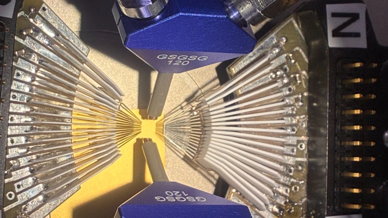
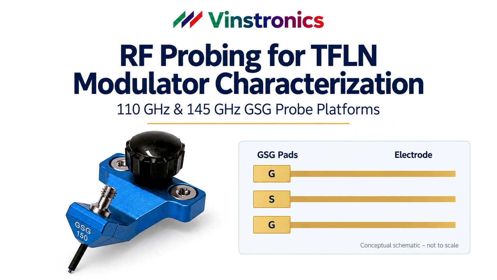
Die-to-die interconnect characterization begins with an accessible electrical path and a clear test boundary. Before measuring, engineers must define which part of the interconnect is under test, how it can be accessed and what the test structure adds to the result.
A multi-chip package may contain redistribution layers (RDLs), microbumps, interposer or bridge routing and vias. Many are inaccessible after assembly, making purpose-designed test structures and defined reference planes essential.
What Is Actually Being Characterized in a Die-to-Die Link?
A die-to-die channel includes transitions as well as routing. Its response depends on materials, geometry, return paths and coupling to neighboring conductors.
Individual interconnect structures
Dedicated coupons can isolate an RDL trace, via transition or die-to-interposer interface. Such structures are useful when validating an electromagnetic model or investigating a particular discontinuity.
Back-to-back test vehicles
A back-to-back (B2B) structure connects two nominally similar transitions through an accessible interconnect. Multiple line lengths and suitable standards can support extraction of the intended transition or line response. The complete measured loss should not simply be divided by two unless the extraction method justifies doing so.
Representative end-to-end channels
A more complete test vehicle can reproduce several transitions and a larger fraction of the intended package routing. This helps correlate measurement with full-wave simulation, although it makes individual effects harder to isolate.
Before comparing insertion loss, document whether the reported network includes the pad launches, access lines and both transitions.
Electrical Measurements That Matter
S-parameters are useful for characterizing an accessible interconnect, but the appropriate quantities depend on the port definition and signal topology.
| Measurement | Engineering purpose | Important qualification |
|---|---|---|
| S11 / reflection | Investigate impedance discontinuities at an accessible port | Depends on reference impedance and calibration plane |
| S21 / transmission | Characterize the forward response between measurement ports | Includes everything between the selected reference planes |
| Time-domain response | Identify and compare discontinuities along the measured path | Resolution depends on measurement bandwidth and processing |
| Crosstalk | Assess coupling between adjacent conductors | Requires relevant aggressor/victim access and terminations |
| Phase / propagation delay | Investigate electrical length and timing characteristics | Reference-plane errors affect interpretation |
| Mixed-mode S-parameters | Analyze differential and common-mode behavior | Only meaningful for appropriately defined differential ports |
Insertion loss and reflections
Insertion and return loss reveal attenuation, discontinuities and resonances. A favorable 50 Ω S21 trace, however, does not establish link performance with the actual transmitter and receiver.
Crosstalk in dense routing
Closely spaced package conductors can couple through the interposer, RDL, return structure or adjacent routing. Crosstalk measurements must define aggressor and victim paths, accessible ports and unused-port terminations. A densely routed interface may require more than an isolated pairwise measurement.
Time-domain interpretation
Time-domain transforms of broadband network data can help locate impedance changes. Apparent feature positions and amplitudes depend on measurement bandwidth, windowing and the selected reference plane; they are not independent of the frequency-domain measurement.
Single-Ended and Differential Signaling Must Be Treated Separately
Die-to-die links do not necessarily carry differential data. In common UCIe PHY arrangements, data lanes are single-ended while forwarded clocking uses paired clock signals; details vary by specification revision and operating mode.
For an accessible single-ended structure, conventional S-parameter measurements can characterize loss, reflections and delay. When its pads are arranged Ground–Signal–Ground, a compatible GSG probe can provide appropriate access.
For a true differential electrical pair, a calibrated multiport network may be converted to mixed-mode parameters such as SDD21 or SDD11. Those measurements require correctly defined differential ports. SDD21 should not be used as a generic replacement for S21 on a single-ended UCIe data lane.
GSG, GSSG and GSGSG are physical contact arrangements; the DUT pads and return path determine their suitability.
Why S21 Alone Is Not Enough for UCIe Channel Evaluation
A VNA often characterizes a network with 50 Ω reference impedance. Those port conditions may differ from the source and receiver of a short-reach PHY.
UCIe specifications use Voltage Transfer Function (VTF) based channel evaluation for relevant insertion-loss and crosstalk requirements. Such calculations depend on the specified source/receiver models and terminations, which can include resistive and capacitive elements. The exact requirements must be taken from the relevant revision, operating mode and package category.
A calibrated network can be a useful input to the appropriate channel simulation. But a single 50 Ω S21 curve—or a high-frequency RF probe—does not demonstrate UCIe PHY compliance. The UCIe Consortium specification resources provide the relevant standards context.
Where Can Engineers Physically Probe a Die-to-Die Interconnect?
Internal microbumps, bonded interfaces and interposer traces may be inaccessible after package assembly. RF access is often built into dedicated wafers, coupons or package test vehicles. The broader differences between wafer, package and board access are covered in our RF probing for advanced packaging guide.
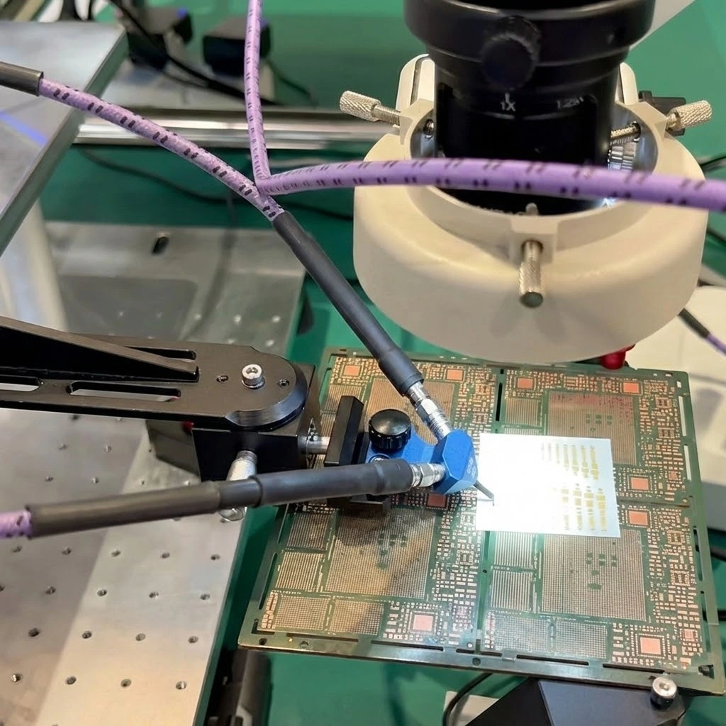
Wafer-level access pads
Dedicated test pads can expose representative lines, transitions and device interfaces before packaging. Pad arrangement, dimensions, spacing and metallization must match the chosen probe’s contact requirements.
Interposer or RDL test coupons
Test coupons may include through lines, multiple trace lengths, back-to-back transitions and aggressor/victim routes. They enable more controlled investigation of structures that would otherwise be difficult to isolate after assembly.
Package test vehicles
Specially designed packages can expose pads or external interfaces connected to internal structures. Additional launch routing between the access point and the desired device boundary must then be characterized or included in the reported network.
Fine-tip contact dimensions do not imply that a probe can directly contact arbitrary microbump arrays. Probe-tip size, contact pitch and the DUT’s usable landing area are different constraints. Representative, accessible test structures are often more practical than attempting to land directly on a functional internal interface.
Calibration, Reference Planes and De-Embedding
A measurement includes the probe path and DUT access structures. The intended reference planes determine which elements remain in the reported network.
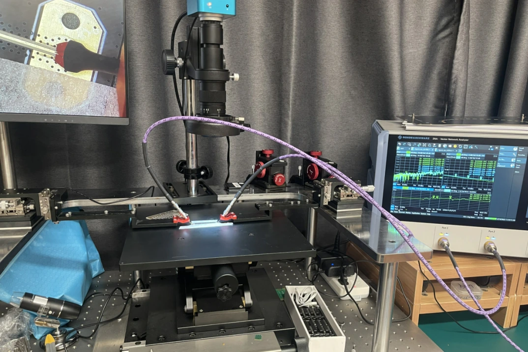
Calibration establishes a reference
A suitable calibration procedure corrects defined systematic errors and establishes electrical reference planes according to the calibration method and standards. A wafer-level calibration may bring the reference toward the probe tips, but it does not automatically remove the DUT’s landing pads or package access structures.
De-embedding isolates the intended structure
If the desired network excludes accessible fixture elements, engineers may use measured fixture networks, suitable reference structures or validated electromagnetic models to remove their contribution. An inaccurate fixture model can generate a plausible-looking result that is not physically reliable. Calibration and de-embedding are complementary, not interchangeable.
A published example of engineered test access
In a 2025 IEEE Transactions on Components, Packaging and Manufacturing Technology study, Erdogan and co-authors characterized interconnects in a die-embedded glass interposer using back-to-back chain structures. Their two-step TRL de-embedding method addressed chip-level and interposer-level lines, with two-port measurements extending to 170 GHz and crosstalk characterization to 50 GHz. Those are the researchers’ measurements—not Vinstronics test results. Read the research overview.
Selecting an RF Probe for Chiplet Test Structures
Select contact geometry from the test structure and its accessible electrical ports.
| Selection item | Question to resolve |
|---|---|
| Test target | Individual transition, RDL line, interposer coupon or end-to-end channel? |
| Contact topology | GS, GSG, GSSG, GSGSG or another accessible arrangement? |
| Pad geometry | Actual pitch, pad dimensions, metallization and landing clearance? |
| Measurement ports | Number of independently accessible ports and return-path arrangement? |
| Frequency range | Bandwidth required by the measurement objective and analysis? |
| Calibration | Available standards and desired electrical reference planes? |
| Use of measured data | Process study, EM correlation, channel model or standards-oriented assessment? |
The AQUILA™ RF probe platform is relevant to compatible wafer-level and fine-pad microwave/mmWave access. A fine probe-tip dimension does not imply an equally fine contact pitch, nor universal compatibility with microbump arrays.
A GSG probe can be appropriate for a matching single-ended coupon; multiport or differential structures may require another contact configuration. The Vinstronics RF probe range provides alternative architectures for appropriately designed wafer- and PCB-oriented test structures. The probe establishes access; it does not replace the test vehicle, measurement instrument or standards methodology.
From Measured S-Parameters to Channel Assessment
A network with defined reference planes can support EM-simulation correlation, transition analysis and channel modeling.
Standards-based PHY assessment additionally requires the specified transmitter/receiver model and evaluation criteria; functional or interoperability testing may also be needed.
Conclusion
A meaningful die-to-die measurement starts with an accessible, representative structure and an explicit reference plane. It must preserve the distinction between a local transition, a back-to-back coupon and an end-to-end channel.
For UCIe work, S-parameters can inform channel models; VTF-based evaluation and compliance require additional prescribed conditions. Measure the intended channel—not just a convenient access path.
Related Engineering Resources
- RF Probing for AI Accelerators, Chiplets and High-Speed Computing
- RF Probing for Advanced Packaging: Wafer, Package and PCB Measurement Challenges
Technical References
- UCIe Consortium — Specifications, relevant electrical-layer and channel-assessment provisions.
- Erdogan, S., Jia, X., Li, X., et al. (2025). Broadband Characterization of Interconnects in Die-Embedded Glass Interposer. IEEE Transactions on Components, Packaging and Manufacturing Technology, 15(4), 766–773. DOI: 10.1109/TCPMT.2025.3548082.
- Vinstronics — AQUILA™ Precision RF Probe Platform, product scope and configurations.
Working on an Accessible High-Frequency Test Structure?
Share the DUT pad layout, signal topology, required frequency range and intended reference plane. Vinstronics can review suitable RF probe contact configurations for your measurement setup.