Thin-film lithium niobate (TFLN) modulators are pushing electro-optic characterization toward and beyond 110 GHz. At these frequencies, delivering a controlled microwave signal to the device’s traveling-wave electrode is a measurement challenge in its own right.
A high-bandwidth electro-optic modulator does not automatically provide an equally broadband electrical interface. Electrode attenuation, reflections, RF-to-optical velocity matching and the probe-to-pad transition all affect the result. For test engineers, choosing an RF probe is therefore part of defining a credible measurement path—not simply matching a frequency number.
Why TFLN Modulators Need High-Frequency RF Access
TFLN Mach–Zehnder modulators use the electro-optic effect of lithium niobate to convert an electrical drive signal into optical modulation. Broadband implementations commonly use traveling-wave electrodes that allow the microwave signal to propagate along the optical waveguide.
Three aspects of the electrode are especially relevant to RF characterization:
- Microwave attenuation: conductor, dielectric and structural losses reduce the RF signal along the electrode as frequency increases.
- Impedance and reflections: the launch, electrode and termination can introduce mismatches, which affect both electrical response and the observed EO transfer function.
- RF–optical velocity matching: a mismatch between the microwave effective index and optical group index can limit usable modulation bandwidth.
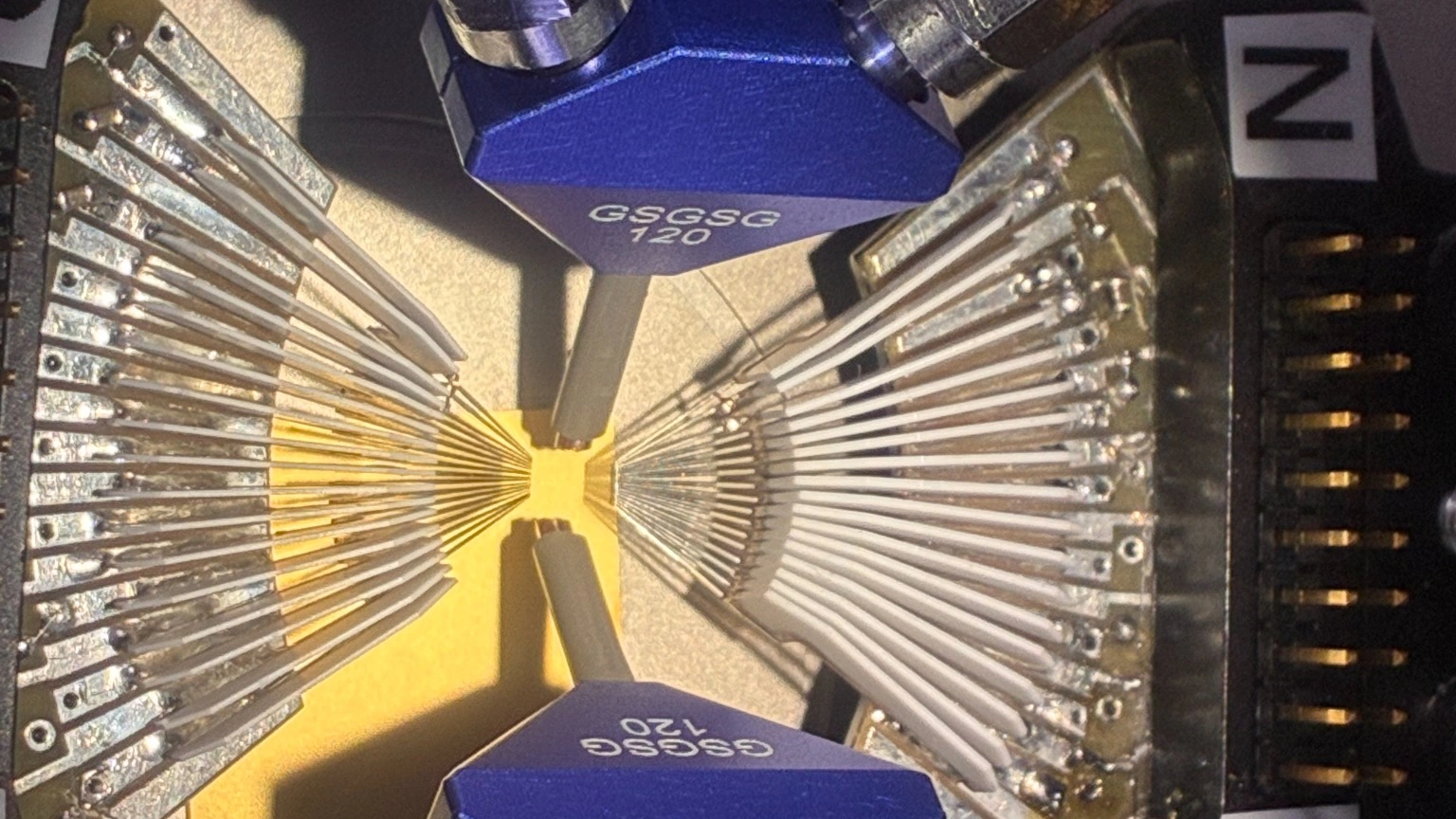
The RF probe establishes electrical access to the device’s pad layout. Its contact transition should be treated as part of the measurement network, particularly when the sweep approaches the upper end of the probe and instrument range.
Electrical S-Parameters Are Not the Same as EO Response
Electrical and electro-optic measurements answer different engineering questions. Both may be reported using an S21-style frequency response, but the physical input and output quantities are not the same.
| Measurement | What it describes | Typical access / setup |
|---|---|---|
| Electrical S11 | Input reflection of the RF electrode and its accessible transitions | VNA and compatible RF probe access |
| Electrical S21 | Microwave transmission through a two-port electrode or test structure | Two-port VNA setup with suitable RF access at both ends |
| EO S21 / EO frequency response | Frequency-dependent conversion from RF drive to optical modulation | RF stimulus, optical input and calibrated optical detection / LCA arrangement |
| Vπ or VπL | Modulation efficiency under specified measurement conditions | Electrical bias/drive and optical characterization; not an RF S-parameter by itself |
For a traveling-wave electrode with accessible RF ports, electrical S11 and S21 help characterize its launch and propagation behavior. EO frequency-response measurement includes the modulator’s optical operation and the optical receiver path, so the setup and normalization have to be considered separately.
The Probe-to-Electrode Transition: Pad Geometry Before GHz Rating
High-speed TFLN electrodes often use coplanar RF layouts. When the test pads are arranged Ground–Signal–Ground, a single-ended GSG RF probe is a logical contact architecture to evaluate.
Probe selection still requires a DUT drawing. The key details include signal and ground pad order, center-to-center pitch, pad dimensions, metallization, approach direction and available mechanical clearance. A 100 μm pitch probe and a 250 μm pitch probe are different configured geometries; one probe does not automatically adjust across the entire available pitch range.
A push-pull optical modulation mechanism should not be taken as proof that the external RF landing requires a GSSG or GSGSG differential probe. The actual electrical pad topology and drive arrangement determine whether a GSG, differential or other configuration is suitable.
Contact repeatability, local ground-return continuity and probe alignment also matter. A nominally compatible contact layout can still introduce an undesirable discontinuity if the probe-to-pad launch is not controlled.
110 GHz Probing in Published TFLN Measurements
High-frequency RF probing is already used in published TFLN characterization. In a 2025 study in Light: Advanced Manufacturing, researchers delivered a small-signal RF input through a 110 GHz probe and measured the modulator’s electro-optic response using a lightwave component analyzer.
The reported EO response showed a roll-off of approximately 2.3 dB at 110 GHz. Because the response had not reached the 3 dB threshold at the upper end of the reported sweep, the authors described the EO 3 dB bandwidth as exceeding 110 GHz. This does not mean the 3 dB cutoff frequency itself was measured above 110 GHz. [1]
A separate TFLN study in Nature Communications used a 110 GHz RF probe and lightwave component analyzer to assess broadband EO response at multiple optical wavelengths, highlighting how electrode impedance, termination and microwave-to-optical index matching affect the result. [2]
These are examples from independent research—not measurements performed or verified by Vinstronics. They establish the engineering relevance of 110 GHz RF electrical access to TFLN devices with compatible RF pads.
Where Vinstronics 110 GHz and 145 GHz GSG Probes Fit
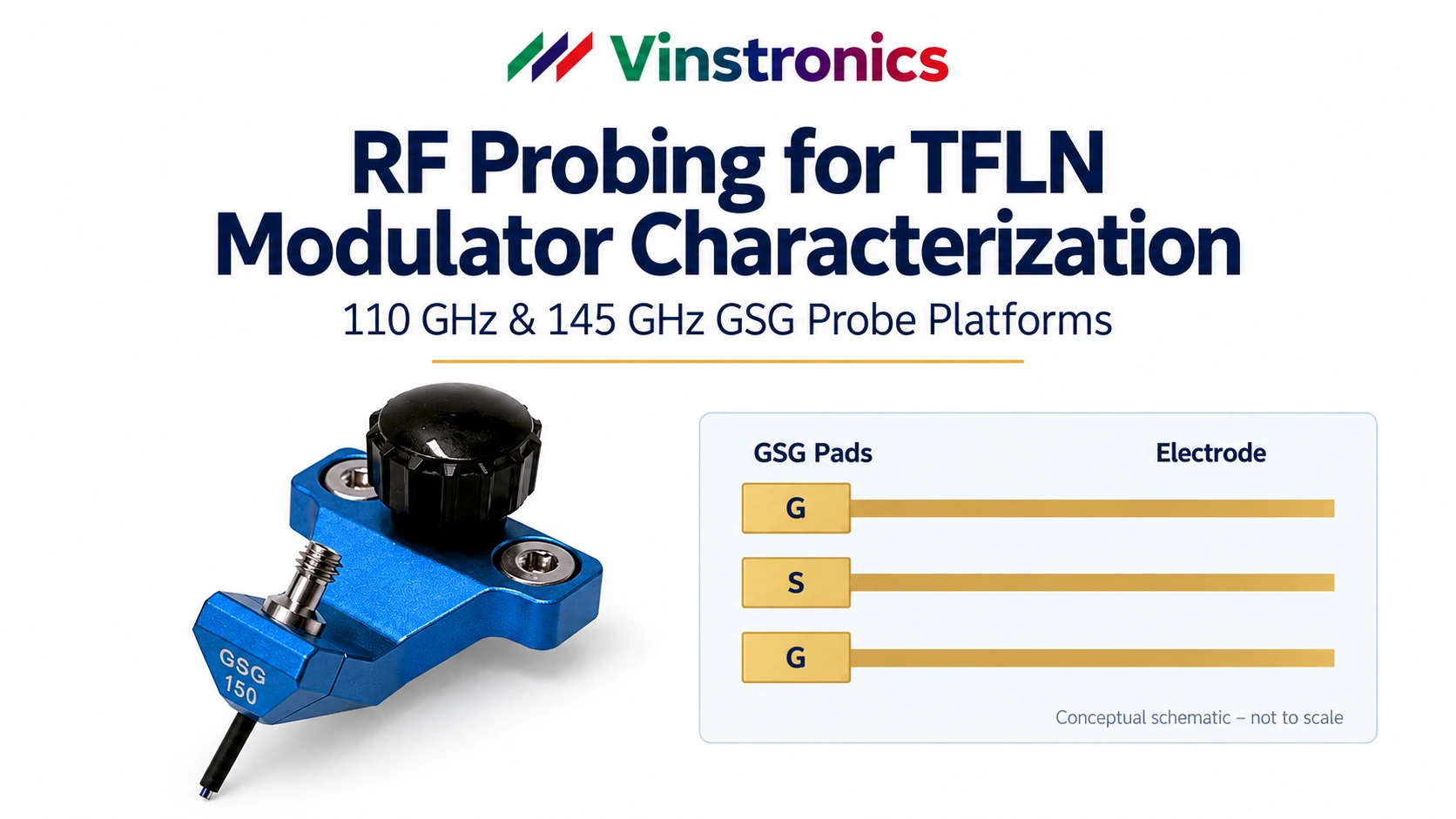
Vinstronics provides GSG probe platforms for wafer and planar device characterization. Their suitability for a particular TFLN modulator depends on the electrode landing geometry, frequency objective and the available instrument-side interface.
| Probe | Rated Frequency | RF Interface | Published Pitch Range |
|---|---|---|---|
| VST-110G-GSG-XXX | DC–110 GHz | 1.00 mm Female | 100–1250 μm |
| VST-145G-GSG-XXX | DC–145 GHz | 0.8 mm Female | 100–1250 μm |
110 GHz: A Practical Electrical-Access Option
The VST-110G-GSG-XXX is a 50 Ω GSG probe with a 1.00 mm female interface. It can be considered for compatible TFLN electrode or test-vehicle layouts when the required RF measurement range extends toward 110 GHz.
145 GHz: Extending the Electrical Measurement Range
The VST-145G-GSG-XXX is a 50 Ω GSG probe rated to 145 GHz with a 0.8 mm female interface. It offers a higher-frequency electrical contact option for a compatible planar DUT and suitable D-band-capable measurement system.
Using a 145 GHz probe does not extend the frequency range of a 110 GHz VNA or lightwave component analyzer. Nor should the probe be presented as proof of a 145 GHz TFLN EO measurement. The usable range is determined by the calibrated system, including instrument, RF interconnects, transitions and DUT access.
Calibration, Termination and the Reference Plane
A representative electrical measurement path is:
On-wafer calibration with suitable standards can establish a defined RF reference plane near the probe-tip contact. Even then, the DUT pad launch and electrode access geometry may remain in the measured network. If the desired reference plane is deeper inside the DUT, additional characterization and appropriately justified de-embedding may be necessary.
Traveling-wave electrode termination also deserves attention. A termination may be integrated on-chip or implemented externally, depending on the device. Its impedance and physical configuration can influence reflections and the observed EO response. It should not be assumed that every TFLN electrode uses an ideal external 50 Ω load.
For EO measurements, optical coupling, the detector or LCA response, optical bias point and normalization method must also be recorded. RF probe calibration does not remove those optical measurement contributions.
A Practical RF Probe Selection Checklist for TFLN Devices
Before requesting a high-frequency probe configuration, provide the DUT layout and intended test setup. The following information allows a more meaningful engineering review than the target frequency alone.
| Item | Information to Confirm |
|---|---|
| Measurement objective | Electrical S11/S21, EO response or both; required upper frequency |
| Pad geometry | GSG or other contact topology, pad pitch, pad size and metallization |
| Mechanical access | Probe approach angle, station clearance and repeatable landing conditions |
| Electrical path | VNA/LCA bandwidth, RF connector, cable and termination arrangement |
| Reference plane | Calibration standards, location of reference plane and de-embedding plan |
With this information, the appropriate 110 GHz or 145 GHz GSG configuration can be reviewed against the actual electrode geometry. A higher frequency rating is useful only when the complete test system can make use of it.
Conclusion
TFLN modulators are extending the frequency range over which RF engineers need reliable wafer-level electrical access. Their traveling-wave electrodes must be considered as microwave structures, with attenuation, impedance, termination and velocity matching contributing to the measured response.
Precision GSG probing can provide an electrical interface to compatible RF pads. The Vinstronics 110 GHz and 145 GHz platforms address different upper-frequency requirements, but neither one independently determines the modulator’s electro-optic bandwidth.
The right RF probe is defined by the electrode geometry, measurement objective and calibrated system—not the frequency rating alone.
Technical References
- Y. Liu et al., “Volume manufacturing of thin-film lithium niobate modulators with bandwidth > 110 GHz based on 4-inch wafer with a quartz handle,” Light: Advanced Manufacturing, 2025. DOI: 10.37188/lam.2025.047.
- “Ultra-broadband near- to mid-infrared electro-optic modulator on thin-film lithium niobate,” Nature Communications, 2026. View article.
- VLC Photonics, “EO Characterization of PIC up to 110 GHz: Methodology and Experimental Results.” Technical application discussion.
Need an RF Probe Matched to Your TFLN Electrode Layout?
Send the electrode pad drawing, pitch, required test frequency and instrument interface. Vinstronics can review the appropriate GSG probe configuration and RF contact requirements.