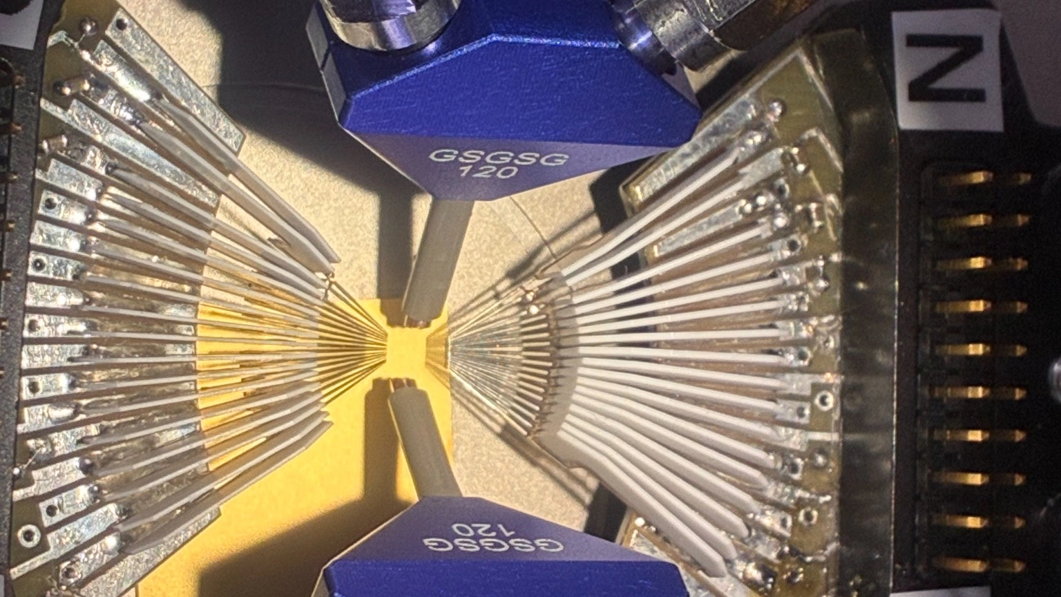
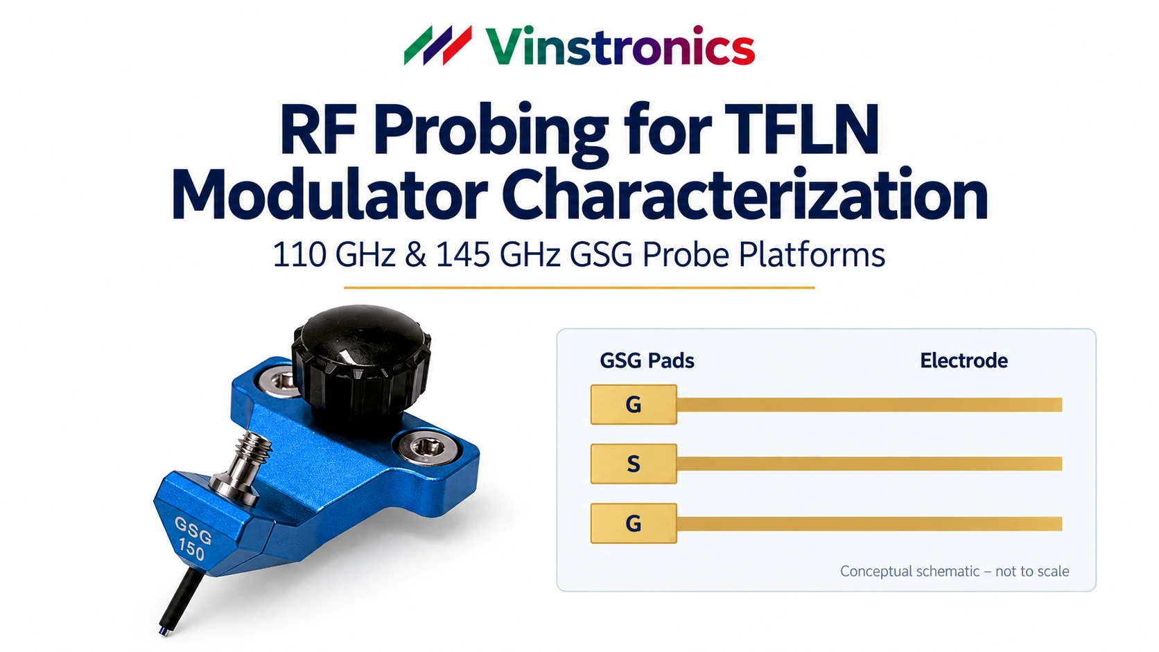
High-speed optical module test boards are becoming demanding RF fixtures in their own right.
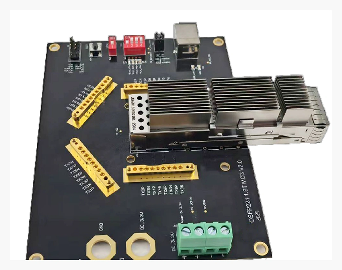
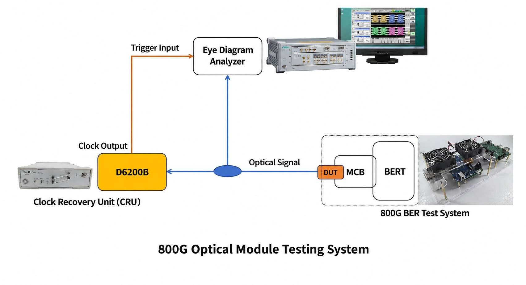
As electrical interfaces move from 800G toward 1.6T and future 3.2T-class systems, the challenge is no longer limited to the optical module itself. Module compliance boards (MCBs), PCB launches, RF connectors, cables, and measurement equipment all become part of the electrical validation path.
For an MCB, the objective is straightforward:
Provide controlled access to each high-speed electrical lane without allowing the fixture to dominate the measurement.
This is where solderless vertical launch connectors can be especially useful.
They allow coaxial RF access to be distributed around the module interface rather than forcing every measurement path to the edge of the PCB.
But connector placement alone does not solve the measurement problem.
As optical-module lane rates increase, PCB launch quality, fixture-channel performance, mechanical installation, calibration, and de-embedding become increasingly important.
Why Optical Module MCBs Need Multiple Coaxial RF Access Points
A module compliance board is more than a breakout PCB.
It forms part of the electrical validation environment between the optical module interface and the measurement equipment.
During development and compliance work, engineers may need access to multiple transmit and receive lanes for transmitter characterization, receiver testing, signal-integrity validation, channel debugging, compliance measurements, and fixture-to-module correlation.
This creates a practical fixture challenge: many high-speed electrical lanes need to be converted into accessible coaxial measurement paths within a limited PCB area.
The challenge becomes more demanding as platforms move from 112G-class electrical lanes toward 224G-class lanes used in 1.6T validation.
The aggregate module rate matters at the system level.
For the fixture designer, however, the more useful question is:
What electrical lane must be measured, and what measurement path is required to characterize it accurately?
That distinction is important when selecting both the RF interface and the test-board architecture.
Why Vertical Launch Fits Many Optical Module Test-Board Architectures
Optical module MCBs often place the module socket or DUT inside the PCB area, with multiple high-speed electrical lanes distributed around it.
In this geometry, routing every measurement path to the outer edge of the board can add trace length, consume routing area, and make the fixture more difficult to organize.
Vertical launch provides another option:
Bring the coaxial measurement interface closer to the electrical point of interest.
This can be particularly useful when many RF access points must surround a module interface.
The advantage is architectural rather than absolute.
Vertical launch does not automatically provide better RF performance than end launch. The final result still depends on the connector-to-PCB transition, transmission-line geometry, PCB stack-up, return path, and complete fixture implementation.
What vertical launch provides is greater freedom in deciding where the coaxial interface is placed.
For dense optical-module MCBs, that can be a significant design advantage.
For a broader discussion of board-level measurement access in high-speed fixtures, see
Vertical Launch Connectors for 112G / 224G SerDes Test Fixtures
.
Why Solderless Mounting Helps During MCB Development
Optical-module fixtures often evolve during development.
A board may be revised as engineers change lane routing, module interfaces, thermal structures, connector locations, or measurement configurations.
A solderless compression-mount RF connector can be removed without desoldering the connector from the PCB.
That can simplify fixture rework, connector replacement, debugging, and development-stage board revisions.
But solderless does not mean variation-free.
Connector seating, alignment, PCB flatness, mounting condition, contact surfaces, and cable loading can still affect the reinstalled RF transition.
Solderless mounting improves serviceability. Measurement repeatability still depends on the installed system.
For more on this issue, see
Solderless Vertical Launch Connector Repeatability: Mounting Force, Alignment, and Reinstallation
.
From 800G to 1.6T: The Electrical Validation Problem Changes
Moving from 800G to 1.6T is not simply a matter of doubling the number printed on the module.
The electrical lane architecture also becomes more demanding.
800G-class systems commonly operate around 112G-class electrical lanes, while 1.6T platforms move electrical validation into the 224G-class lane range.
At these higher lane rates, the fixture becomes more sensitive to insertion loss, reflections, launch discontinuities, channel asymmetry, calibration stability, and fixture-to-fixture variation.
The MCB can therefore consume a larger portion of the available measurement margin if its RF behavior is not well controlled.
At higher lane rates, the compliance board must be treated as part of the measurement system—not as a passive carrier for the DUT.
Toward 3.2T: Fixture Requirements Will Continue to Tighten
The industry is already evaluating electrical interfaces beyond today’s 224G-class lanes.
Future 3.2T-class systems are expected to push test platforms toward still higher electrical bandwidth and denser validation architectures.
The exact implementation will continue to evolve, and 3.2T should still be treated as a next-generation validation direction rather than simply an extension of today’s mature 800G test environment.
What is already clear is that the fixture cannot be separated from this evolution.
As electrical interfaces move toward future higher-per-lane bandwidths, the tolerance for fixture-induced loss, reflection, and uncertainty becomes smaller.
That does not mean the answer is simply to install a higher-frequency connector.
The complete measurement access path must evolve together.
Module Data Rate Does Not Specify the RF Connector Interface
One of the easiest mistakes is to map module generations directly to RF connector families.
For example:
800G → one connector
1.6T → another connector
3.2T → a still higher-frequency connector
That is not a reliable engineering selection method.
Module data rate does not directly specify the RF connector interface.
Connector selection should instead follow the actual measurement requirement.
Electrical Lane Rate → Symbol Rate → Required Measurement Bandwidth → Fixture Loss / Reflection Budget → Calibration / De-Embedding
The same module generation may use different RF access architectures depending on what is being measured, how much bandwidth is required, what instrumentation is available, and how the fixture is constructed.
Connector frequency rating should therefore be treated as one element of the measurement architecture—not as a direct translation of aggregate module throughput.
The MCB Launch Is Part of the Measurement Channel
Once the coaxial signal enters the PCB, the measurement no longer depends on the connector alone.
A vertical-launch MCB path may include:
Coaxial Connector → PCB Launch → Trace / Via Transition → Module Electrical Interface
The connector contact, landing structure, PCB ground return, transmission line, vias where applicable, and module interface all contribute to the measured response.
A 40 GHz, 50 GHz, or 67 GHz connector does not automatically create an MCB with equivalent usable bandwidth.
The connector and PCB launch need to work together.
This is why a high-speed optical-module test board should not treat the RF connector as a mechanical component added after the PCB routing is already complete.
The launch belongs to the measurement channel.
For a deeper discussion of this transition, see
How PCB Launch Geometry, Ground Vias, and Return Path Affect Vertical Launch Connector Performance
.
Calibration and Fixture Characterization Matter More as Lane Rates Increase
An electrical validation instrument measures through everything between its calibrated reference plane and the signal point of interest.
That path may include test cables, RF connectors, PCB launches, fixture traces, vias, and adapters.
At higher lane rates, the contribution of these structures becomes harder to ignore.
For an optical-module MCB, engineers therefore need to understand:
Where is the measurement reference plane?
How much of the MCB is included in the result?
Does the fixture need to be characterized or de-embedded for the intended measurement?
The answer depends on the validation objective.
A development or debug board, a compliance fixture, and a production screening platform may not require the same level of fixture characterization.
Convenient coaxial access is not automatically transparent measurement access.
Engineering Checklist for an Optical Module Test Board
Before releasing an MCB or other high-speed optical-module validation fixture, review the complete measurement path.
-
Electrical lane architecture
What lane rate and symbol rate must be characterized? -
Measurement objective
Is the fixture intended for compliance testing, transmitter characterization, receiver testing, debugging, correlation, or production validation? -
RF access location
Are the measurement points near the PCB edge, or are they distributed around the module interface? -
Connector interface
Does the selected RF interface provide appropriate bandwidth and mechanical integration for the actual measurement? -
PCB launch
Has the connector-to-board transition been reviewed for the actual PCB stack-up and routing structure? -
Fixture channel
Are PCB trace loss, discontinuities, cable loss, and channel symmetry acceptable for the measurement objective? -
Mechanical repeatability
If connectors can be removed and reinstalled, is the installation procedure controlled? -
Calibration / fixture removal
Where is the measurement reference plane, and how will fixture effects be handled?
The central design question should not be:
“Which connector is used for a 1.6T module?”
It should be:
“What measurement path is required for the electrical lane being characterized?”
Optical Module Testing Is Becoming a System-Level Interconnect Problem
The progression from 800G toward 1.6T and future 3.2T-class optical systems is increasing the demands placed on electrical validation fixtures.
The MCB, RF connector, PCB launch, cable, calibration method, and instrument are no longer independent decisions.
They form one measurement chain.
Solderless vertical launch connectors can be valuable in this environment because they provide distributed coaxial access around the module interface while supporting serviceable development fixtures.
But they still need to be evaluated as part of the complete RF path.
As optical modules move from 800G to 1.6T and toward 3.2T, fixture bandwidth, launch integrity, calibration, and measurement access must evolve together.
For available Vinstronics 1.0 mm, 1.85 mm, 2.4 mm, and 2.92 mm solderless vertical launch configurations, see the
Solderless Vertical Launch PCB Connectors
platform.
Discuss Your Optical Module Test Fixture Requirements
If you are developing an optical-module compliance board, electrical validation board, or other high-speed module test platform, useful information for an engineering review includes the module electrical interface, lane rate and symbol rate, required measurement bandwidth, number and location of RF access points, PCB stack-up, routing architecture, preferred RF connector interface, cable and instrument configuration, and intended calibration or de-embedding approach.
This allows the RF connector and optical-module test board to be reviewed as part of the complete measurement path.