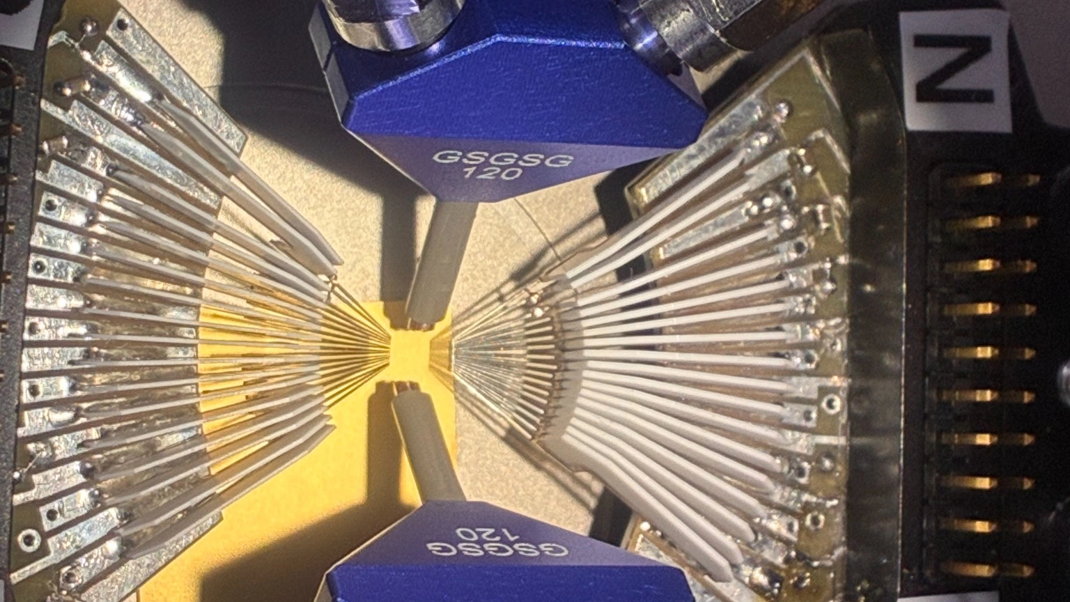
In many 112G and 224G SerDes validation fixtures, the biggest challenge is not selecting the connector with the highest frequency rating.
The real challenge is creating a controlled and repeatable RF access point at the location where the high-speed channel actually needs to be measured.
As data rates continue to increase, engineers must consider more than the connector itself. The RF transition includes the measurement point, PCB launch structure, connector interface, fixture architecture and calibration reference plane.
High-speed fixture design should start with the measurement requirement, not with the connector selection.
A typical RF measurement path can be viewed as:
Measurement Point → PCB Launch → Connector Interface → Cable / Instrument → Calibration Reference
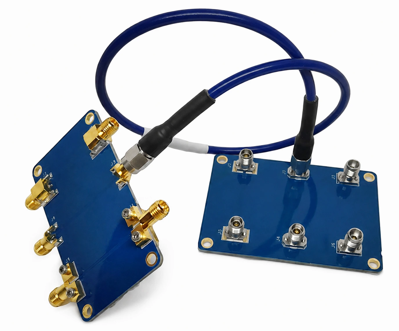
Solderless vertical launch connectors provide one solution for this challenge by allowing coaxial measurement access directly at the required PCB location instead of forcing every test path to the board edge.
This design approach is especially relevant for high-speed evaluation boards, optical module compliance boards, SerDes validation fixtures and signal-integrity characterization platforms.
For available configurations, see the Vinstronics
Solderless Vertical Launch PCB Connectors
series.
Why RF Access Location Matters in High-Speed SerDes Testing
In a traditional PCB test setup, engineers often prefer edge-mounted connectors because they provide straightforward cable access.
However, modern high-speed designs do not always place the desired measurement point near the PCB edge.
For 112G and 224G SerDes validation, measurement access may be required near:
- ASIC or FPGA interfaces;
- optical module electrical interfaces;
- specific channel segments;
- transmitter or receiver observation points;
- reference structures used for fixture characterization.
When the measurement location is physically inside the PCB area, routing the signal all the way to the edge only to accommodate an RF connector can introduce unnecessary design constraints.
The additional routing length may affect:
- signal path loss;
- impedance continuity;
- return-current path;
- fixture layout flexibility;
- accessibility during validation.
The purpose of a vertical launch architecture is therefore not simply to achieve higher frequency performance. Its main advantage is providing a controlled RF access point where the engineer needs to observe the channel.
Vertical Launch vs. Edge Access: Choosing the Right Measurement Point
Both edge-launch and vertical-launch approaches can be appropriate depending on the fixture architecture.
Edge Launch
Measurement point → PCB routing → board edge → coaxial connector
Vertical Launch
Measurement point → local PCB transition → coaxial connector
An edge-launch solution can be ideal when the signal naturally reaches the PCB edge and the mechanical layout supports side access.
A vertical launch solution becomes attractive when the required measurement point is located away from the edge or when multiple RF access points must be distributed around the DUT area.
The correct selection should follow the measurement architecture:
Choose the RF access method according to where the signal needs to be measured, not where the connector is easiest to place.
For a detailed comparison between these two PCB interface approaches, see:
End Launch vs. Vertical Launch RF Connectors for PCB Testing
.
Connector Bandwidth Is Only One Part of the RF Transition
One common misunderstanding in high-speed SerDes testing is selecting the RF interface directly from the data-rate label.
For example:
112G ≠ automatically one connector type
224G ≠ automatically another connector type
The required connector bandwidth depends on the actual measurement objective, not only the digital signaling rate.
Different validation tasks may require different measurement bandwidths, including:
- S-parameter characterization;
- channel insertion-loss evaluation;
- return-loss measurement;
- fixture characterization;
- transmitter or receiver validation;
- de-embedding and reference-plane definition.
The connector is only one element in the complete RF transition:
Connector → PCB Launch → Fixture → Cable → Instrument → DUT
For this reason, a higher-frequency connector does not automatically create a higher-performance fixture.
The complete measurement chain must be considered together.
If the main design question is whether a test system should remain with a 40 GHz interface or move toward a 67 GHz interface, see our related article:
1.85 mm vs. 2.92 mm Vertical Launch Connectors for High-Speed PCB Testing
.
Designing the PCB Launch for High-Speed Measurement
At higher signaling speeds, the connector itself is only one part of the electrical transition.
The PCB launch structure between the connector and the transmission line becomes an important part of the measured response.
A typical vertical launch transition includes:
Connector Contact → Signal Pad → Ground Structure → Via Field → Transmission Line
Each section can influence insertion loss, return loss and measurement repeatability.
Important PCB design considerations include:
- signal pad geometry;
- ground pad arrangement;
- via and return-current structure;
- PCB stack-up;
- transmission-line type, such as microstrip or grounded coplanar waveguide;
- mechanical alignment between connector and PCB transition.
A high-frequency connector does not automatically create a high-frequency fixture.
The final performance depends on the complete transition between the measurement instrument and the DUT.
The connector, PCB launch and fixture design should be evaluated as one RF structure.
This is especially important for 112G and 224G-class validation, where available channel margin becomes increasingly limited and small discontinuities can affect measurement confidence.
Example: 400G Optical Module Compliance Board Applications
Optical module compliance boards are a typical example where vertical RF access becomes valuable.
High-speed module interfaces may require multiple measurement ports around the module area rather than a single connection point at the PCB edge.
In this type of architecture, vertical launch connectors allow engineers to place RF access points close to the electrical interface being evaluated.
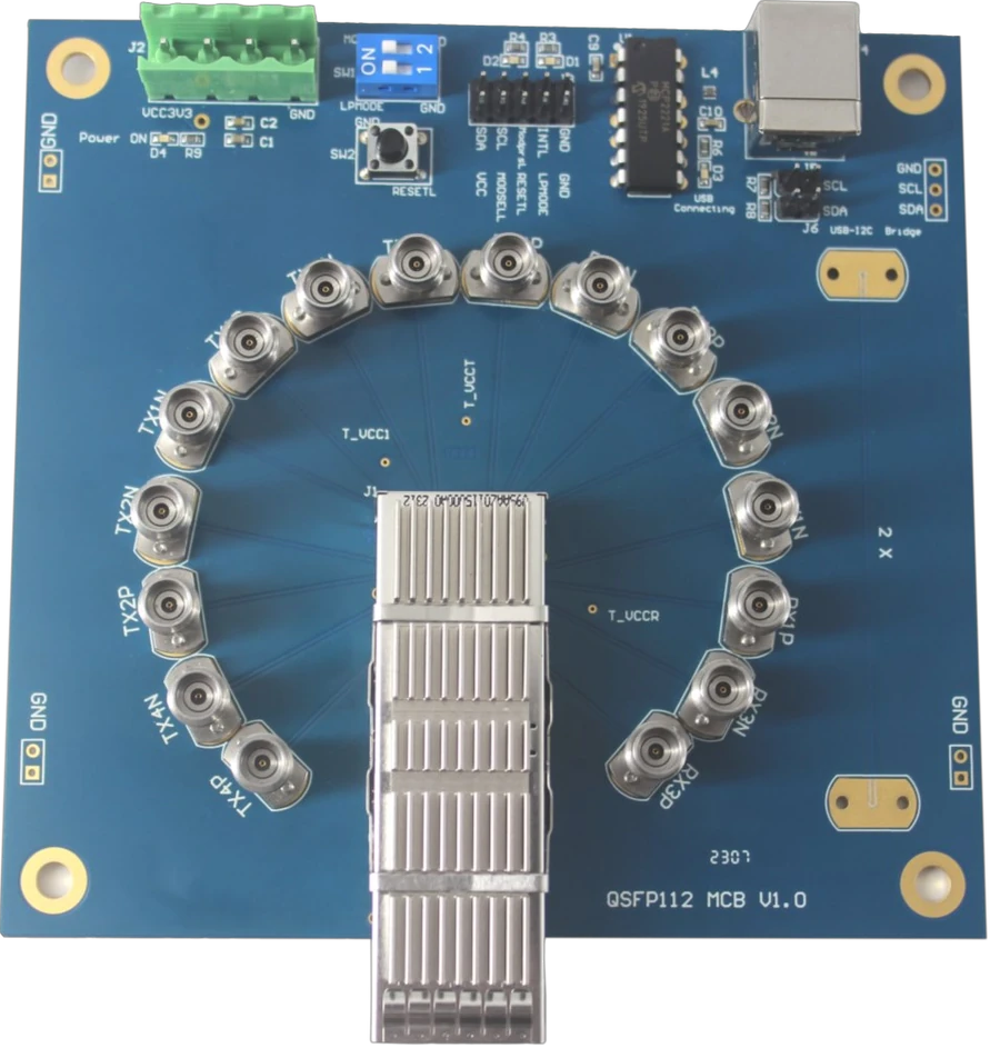
The QSFP112 400G compliance board example demonstrates a common requirement in high-speed validation: multiple RF measurement points need to be positioned close to the DUT rather than routed to a common PCB edge.
The connector selection should then follow the required measurement bandwidth, fixture architecture and instrumentation environment.
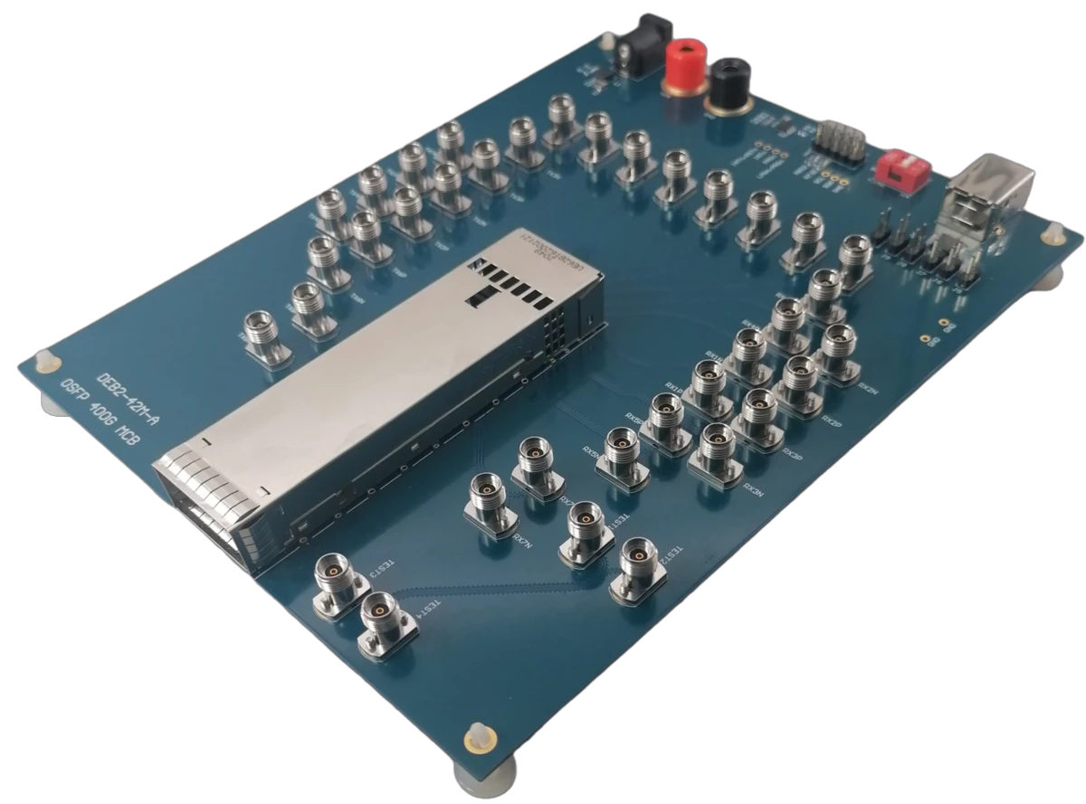
The OSFP 400G example also highlights an important engineering point:
Vertical launch architecture and connector bandwidth are related but separate design decisions.
The vertical launch approach determines how RF access is created on the PCB, while the connector interface selection depends on the required measurement bandwidth and the overall test environment.
This distinction allows engineers to evaluate 1.85 mm, 2.92 mm or other RF interfaces based on actual validation requirements rather than applying a single rule based only on SerDes data rate.
Fixture Calibration and Repeatability
A high-speed measurement fixture is not only an electrical structure. It is also a mechanical system that must provide consistent results during development and validation.
During fixture development, engineers often repeat the following process:
Install → Measure → Modify → Reinstall → Compare
For this reason, the ability to remove and replace a connector without permanently soldering it to the PCB can be valuable during fixture development.
However, solderless mounting should not be interpreted as automatic measurement repeatability.
Repeatable performance still depends on:
- controlled mounting force;
- mechanical alignment;
- PCB surface condition;
- connector positioning;
- consistent installation procedure.
The mechanical interface becomes part of the RF measurement system when the fixture is repeatedly installed, modified and characterized.
Calibration and De-Embedding Considerations
The measurement result obtained from a high-speed fixture includes more than the DUT itself.
Instrument → Cable → Connector → PCB Launch → Fixture → DUT
Engineers must define where the desired measurement reference plane should be located and determine which portions of the fixture need to be characterized or removed through de-embedding.
Important considerations include:
- calibration method;
- reference-plane definition;
- fixture characterization;
- connector transition behavior;
- repeatability of the measurement setup.
A vertical launch connector does not eliminate fixture effects by itself.
Its value is providing a controlled and repeatable RF interface that can be integrated into a properly characterized measurement structure.
Selecting a Vertical Launch Connector for 112G / 224G Validation
Selecting a vertical launch connector for a high-speed SerDes fixture should be based on the complete measurement requirement rather than the data-rate label alone.
Before finalizing the interface, engineers should review several key factors:
- required measurement bandwidth;
- location of the measurement point;
- PCB stack-up and transmission-line structure;
- fixture architecture;
- instrument and cable interface compatibility;
- calibration and de-embedding strategy;
- mechanical access requirements.
For example, a fixture designed for measurements within the 40 GHz range may be appropriately served by a 2.92 mm interface, while a fixture requiring additional bandwidth margin may benefit from a 1.85 mm interface.
The final decision should be made after evaluating the complete RF path rather than the connector specification in isolation.
The best connector choice is the one that supports the required measurement objective with the correct RF and mechanical environment.
Vinstronics provides solderless vertical launch connector solutions across multiple RF interface sizes, including 1.0 mm, 1.85 mm, 2.4 mm and 2.92 mm configurations for high-speed PCB testing and measurement applications.
Engineering Checklist Before Selecting a Vertical Launch Connector
Before integrating a vertical launch connector into a 112G or 224G SerDes test fixture, consider the following questions:
-
Where is the measurement point?
Is the required RF access located at the PCB edge or inside the DUT area? -
What frequency range must actually be characterized?
Select the interface according to the measurement requirement, not only the digital data rate. -
What bandwidth margin is required?
Consider future validation requirements and fixture reuse. -
What PCB structure will be used?
Review stack-up, transmission-line type, pad geometry and grounding structure. -
How will the fixture be calibrated?
Define the measurement reference plane and de-embedding approach. -
What mechanical requirements exist?
Consider mounting area, connector replacement needs and installation repeatability.
Reviewing these factors early helps avoid selecting a connector that does not match the actual measurement architecture.
Frequently Asked Questions
Do 112G or 224G SerDes fixtures always require 1.85 mm vertical launch connectors?
No. The SerDes data rate alone does not determine the connector interface. The appropriate connector depends on the required measurement bandwidth, fixture architecture and instrument environment.
Why use a vertical launch connector instead of an edge-launch connector?
A vertical launch connector allows RF access directly at the required PCB location. This can be useful when the measurement point is located inside the board area or when multiple RF access points are required around the DUT.
Does a higher-frequency connector automatically create a higher-performance test fixture?
No. The connector is only one part of the RF transition. PCB launch design, grounding structure, transmission line, calibration method and fixture repeatability all influence final measurement performance.
Are solderless vertical launch connectors suitable for reusable test fixtures?
Solderless mounting can simplify connector replacement during fixture development. However, repeatable measurement still requires controlled mechanical installation, alignment and PCB launch design.
What information should be provided when selecting a vertical launch connector?
Useful information includes target frequency range, PCB stack-up, transmission-line structure, measurement location, available mounting area, instrument interface and intended validation method.
Discuss Your High-Speed Test Fixture Requirements
If your 112G or 224G-class test platform requires board-level RF access, provide the target bandwidth, PCB stack-up, measurement location and fixture requirements.
Vinstronics can help review the suitable vertical launch interface and provide engineering support for high-speed PCB test fixture development.
Related Articles:
Solderless Vertical Launch PCB Connectors
1.85 mm vs. 2.92 mm Vertical Launch Connectors for High-Speed PCB Testing
End Launch vs. Vertical Launch RF Connectors for PCB Testing