
Solderless Vertical Launch PCB Connectors
DC to 110 GHz, 50 Ω interfaces for high-frequency PCB characterization, high-speed digital validation, optical module testing and precision RF/mmWave test fixtures.

Why Vertical Launch?
Vertical launch provides direct coax-to-board access at the required PCB location without relying on a board-edge transition.

Direct PCB Access
RF access at interior board locations where an edge-launch interface is impractical or restricted.
Compact High-Frequency Transition
A short coax-to-board path reduces unnecessary routing length and helps manage transition discontinuities in high-frequency test structures.
Solderless & Field-Replaceable
Compression mounting enables installation and replacement without permanently soldering the connector to the PCB.
Flexible PCB Integration
Supports microstrip, GCPW and multilayer launch structures matched to the PCB design.
Precision RF Interface Series
Available in 1.0 mm, 1.85 mm, 2.4 mm and 2.92 mm interfaces for high-frequency PCB test and characterization from DC to 110 GHz.

1.85 mm Vertical Launch
High-bandwidth PCB access for optical module, SerDes, semiconductor characterization and precision RF test platforms.
View 1.85 mm Solutions →
2.92 mm Vertical Launch
Versatile PCB access for RF, high-speed digital and general-purpose test fixtures.
View 2.92 mm Solutions →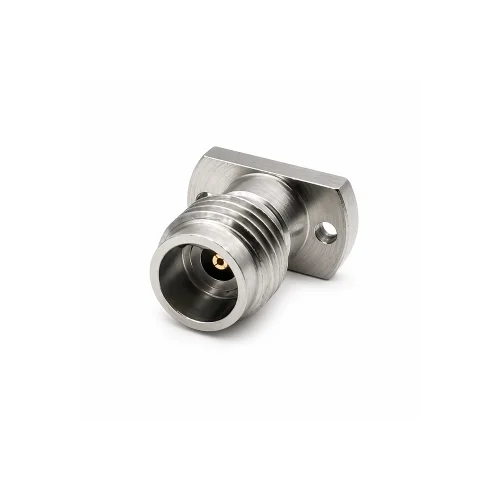
2.4 mm Vertical Launch
For signal-integrity and microwave characterization requiring bandwidth to 50 GHz.
View 2.4 mm Solutions →
1.0 mm Vertical Launch
The highest-frequency interface in the range for mmWave, W-band and advanced high-frequency characterization.
View 1.0 mm Solutions →High-Speed Test Applications
Typical applications span optical module, SerDes, semiconductor, signal-integrity and high-speed interconnect test platforms.

Optical Module Test
High-density RF access for 400G / 800G OSFP and QSFP-DD module compliance and electrical characterization platforms.
SerDes & Semiconductor Test
Board-level RF access for high-speed SerDes, ASIC / FPGA characterization, evaluation boards and semiconductor test fixtures.
Signal Integrity Test
Precision interfaces for differential channel characterization, insertion-loss evaluation, stressed-eye testing and receiver validation.
High-Speed Interconnect Test
RF test access for high-bandwidth PCB, cable and interconnect characterization in data-center and high-performance computing systems.
Technical Selection Matrix
Compare the four precision interfaces by frequency coverage and typical test positioning.
| RF Interface | Frequency Range | VSWR (Typ.) | Typical Test Focus |
|---|---|---|---|
| 1.85 mm | DC–67 GHz | 1.25:1 | High-speed digital & optical module testing |
| 2.92 mm | DC–40 GHz | 1.15:1 | RF & high-speed PCB characterization |
| 2.4 mm | DC–50 GHz | 1.20:1 | Signal integrity & microwave characterization |
| 1.0 mm | DC–110 GHz | 1.30:1 | mmWave & advanced high-frequency characterization |
Common Selection Questions
Why use vertical launch connectors for 112G and 224G SerDes test fixtures?
Vertical launch provides short, direct RF access at the required PCB location without routing the signal to the board edge. This can simplify high-speed test-fixture design and help manage transition length, routing density and serviceability in 112G-class and next-generation 224G SerDes characterization platforms.
How do I choose between 2.92 mm, 2.4 mm, 1.85 mm and 1.0 mm?
Start with the required measurement bandwidth and test environment. 2.92 mm covers applications to 40 GHz, 2.4 mm to 50 GHz, 1.85 mm to 67 GHz and 1.0 mm to 110 GHz. PCB geometry, available mounting area and the measurement-equipment interface should also be considered.
What PCB information is needed for connector selection?
Board thickness, stack-up, transmission-line structure, signal layer, available mounting area and target frequency are the most useful starting points. Vinstronics can review these inputs and recommend a suitable interface and launch configuration.
How is repeatable compression mounting maintained?
Repeatability depends on controlled mounting force, PCB geometry, surface condition and proper mechanical alignment. Following the specified mounting procedure helps maintain a consistent connector-to-board interface during installation and replacement.
Engineering Review for Vertical Launch Integration
Send your target frequency, preferred RF interface and PCB information for connector selection, launch review and quotation support.