A connector rated to 40 GHz or 67 GHz does not automatically create a 40 GHz or 67 GHz PCB launch.
Once a vertical launch connector is installed, the connector becomes only one part of the measured RF structure. The signal contact, PCB landing pad, ground structure, reference planes, and transmission line all participate in the transition. If board-level return loss is worse than expected, an unexpected resonance appears, or the same connector behaves differently on another PCB stack-up, the connector itself may not be the limiting element.
The assembled connector-to-board transition should be reviewed as a whole.
Connector capability and assembled PCB launch performance are not the same specification.
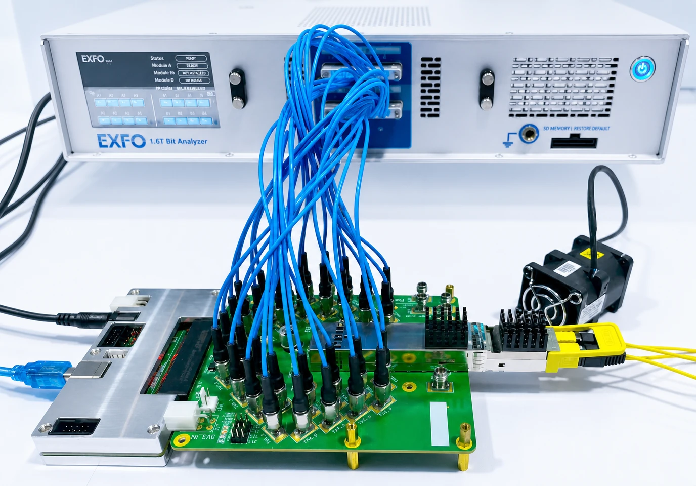
In a complete measurement system, the PCB launch sits between the RF connector and the transmission structure being characterized. Its behavior therefore contributes directly to the measurement path.
For a broader discussion of how these access points are used in high-speed validation, see
Vertical Launch Connectors for 112G / 224G SerDes Test Fixtures
.
The PCB Launch Is One RF Structure
A coaxial connector provides a controlled electromagnetic environment up to the PCB interface. At the board, however, the field must transition from coaxial geometry into a planar transmission-line structure. That transition is not electrically invisible.
Connector Contact → Landing / Signal Pad → Ground / Return Structure → PCB Trace or Via Transition → Transmission Line
The exact path depends on the PCB architecture. A top-layer microstrip or grounded coplanar waveguide launch may transition directly into the PCB trace, while a design that routes the signal to another layer introduces an additional signal-via transition.
In either case, the signal encounters changes in conductor geometry, dielectric environment, and return-current distribution over a relatively short physical distance. At higher frequencies, small discontinuities can contribute measurable capacitance, inductance, and reflection.
This is why connector selection and PCB layout should not be treated as unrelated design tasks. A nominally 50 Ω connector does not guarantee a well-matched 50 Ω transition once the electromagnetic field enters the PCB launch.
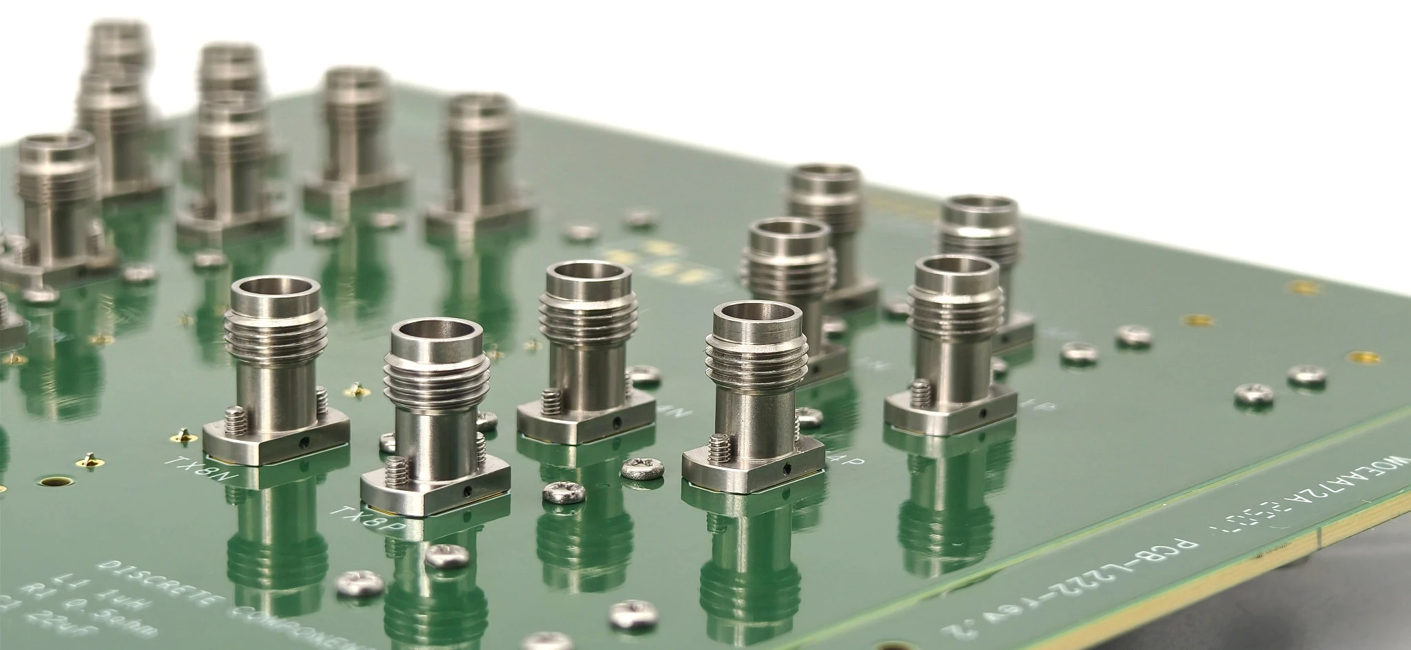
For solderless vertical launch connectors, this interaction is particularly important because the contact interface, landing pad, and surrounding ground structure occupy the same compact launch region. The assembled connector-to-board transition is the RF structure that ultimately needs to perform.
Signal Pad Geometry and Local Impedance
The signal pad is one of the first PCB features encountered after the connector contact. Its size and shape can affect the local impedance of the launch.
A landing pad that is substantially wider than the adjoining transmission line can add local capacitance, while an abrupt change between the connector contact region and the trace can create an impedance discontinuity. The objective is therefore not simply to provide enough copper for reliable mechanical contact. The landing geometry must also support a controlled transition into the PCB transmission line.
A footprint that performs well on one PCB stack-up should not automatically be assumed to behave identically on another.
For example, changing the distance between the top-layer signal pad and its reference plane changes the electric-field distribution around the pad. The top-layer copper can remain unchanged while the electrical behavior of the launch changes.
The same principle applies when moving between transmission-line structures such as microstrip and grounded coplanar waveguide.
Where the launch includes a signal via or an opening in the reference plane, plane-clearance or anti-pad geometry also becomes part of the impedance transition. Changing this clearance changes the local electromagnetic environment, so the top-layer footprint should be reviewed together with the planes and voids beneath it.
The correct landing geometry therefore depends on more than the connector drawing alone. It should be evaluated together with the PCB stack-up, transmission-line geometry, reference-plane structure, and target measurement bandwidth.
There is no universal pad or anti-pad dimension that optimizes every vertical launch application.
Ground Vias and Return-Path Continuity
High-frequency current does not travel only through the signal conductor. The return current is part of the same electromagnetic structure.
Inside a coaxial connector, the center conductor and outer conductor form a controlled signal-and-return geometry. When that field reaches the PCB, the return current must transfer into the board’s ground structure.
Ground vias are an important part of that transition. Their purpose is not simply to provide more ground connections; they help establish a short, controlled path between the connector ground region and the relevant PCB reference planes.
If the effective return path is located too far from the signal transition, the launch may exhibit higher inductive discontinuity and poorer impedance control. A strongly asymmetric ground structure can also alter the local field distribution.
Ground-via placement, spacing, symmetry, and—where applicable—via-ring geometry are critical to launch performance; simply increasing the via count does not guarantee improvement.
Why Via Placement Matters More Than Via Count
It is common to respond to a grounding concern by adding more vias. That may help in some cases, but it is not a complete design strategy.
A ground via positioned near the region where return current naturally needs to flow may contribute more effectively than several vias placed farther away. Symmetry also deserves attention: if one side of the launch has a substantially different ground-via arrangement from the other, the electromagnetic environment around the signal transition changes accordingly.
In via-based launches, the signal via and surrounding ground-via structure can behave as part of a coaxial-like transition. At sufficiently high frequencies, the geometry of this structure can also influence higher-order-mode behavior and the usable bandwidth of the launch.
The signal-via structure can introduce its own limitations as well. Residual via stubs can add parasitic capacitance and may introduce resonant behavior, reducing the usable bandwidth of the transition.
This does not mean every design requires one particular via spacing, diameter, count, or ground-ring pattern. Those values depend on the connector geometry, PCB stack-up, routing layer, and target bandwidth.
The useful engineering principle is that via design should follow the electromagnetic transition rather than a generic rule such as “more ground vias are always better.”
PCB Stack-Up Changes the Launch
The PCB stack-up is part of the launch geometry. Reference-plane depth, dielectric thickness, dielectric properties, and transmission-line construction all affect the electromagnetic environment around the connector.
A signal pad located close to a reference plane does not behave the same way as an identical pad above a substantially deeper plane. Likewise, a grounded coplanar structure does not distribute the field in exactly the same way as a conventional microstrip.
This explains why the same connector and nearly identical top-layer copper can produce different measured results on two different boards. The artwork may look similar, but the RF structure underneath it is not.
Board thickness and layer placement can also matter, especially when the signal transitions to an internal routing layer or when the connector contact geometry is designed around a specific PCB construction.
For higher-bandwidth fixtures, the connector footprint should therefore be reviewed against the actual stack-up rather than copied independently of it.
A reference footprint is a starting point. The final launch belongs to the specific PCB.
What Poor PCB Launch Performance Can Look Like
A poorly controlled launch does not always fail in an obvious way. The connector may install correctly and the DC connection may appear normal while the high-frequency response shows a problem.
Typical symptoms can include:
- worse-than-expected return loss;
- higher insertion loss than expected;
- a localized resonance, notch, or rapid change in response;
- performance that degrades faster than expected with frequency;
- different results when the same connector is integrated into another PCB stack-up;
- poor correlation between connector-level data and assembled fixture measurement.
These symptoms do not automatically indicate a defective connector. They may originate from the connector-to-PCB transition.
Excess local capacitance around the landing pad or plane clearance can create an impedance discontinuity. An inadequate return structure can add inductive behavior. A via or stub structure may introduce unwanted resonant behavior. In practice, several effects can interact.
That is why troubleshooting should begin with the complete launch rather than replacing the connector immediately.
Did the problem originate in the connector, or did it appear after the connector became part of this specific PCB structure?
That distinction often changes where the engineering effort should be focused.
40 GHz and 67 GHz Interfaces Still Depend on the PCB Launch
The same principle applies when choosing between interfaces such as 2.92 mm and 1.85 mm.
A 2.92 mm interface is commonly used in measurement environments extending to 40 GHz, while a 1.85 mm interface provides additional bandwidth for systems extending toward 67 GHz.
But moving from 2.92 mm to 1.85 mm does not automatically improve the PCB launch.
The higher-frequency connector increases the available interface bandwidth. It cannot correct an unsuitable landing pad, discontinuous return structure, poorly controlled plane clearance, or problematic via transition.
This becomes important when upgrading a fixture. An engineer may replace a 2.92 mm connector with a 1.85 mm interface expecting the entire measurement path to improve. If the PCB launch was already the limiting structure, the expected improvement may not appear.
More connector bandwidth does not automatically create more assembled PCB bandwidth.
The correct question is not simply which connector has the higher frequency rating. It is whether the complete measurement path requires the additional bandwidth and whether the PCB transition can preserve it.
For the connector-selection side of this decision, see
1.85 mm vs. 2.92 mm Vertical Launch Connectors for High-Speed PCB Testing
.
That discussion focuses on choosing the RF interface. This article addresses what happens after the selected interface reaches the PCB.
When Simulation and Measurement Are Worthwhile
Reference layouts can provide a useful starting point, particularly when the new PCB closely matches the construction for which the reference launch was developed.
As the required bandwidth increases, however, simulation and measurement become more valuable.
For higher-bandwidth launches, 3D full-wave electromagnetic simulation is commonly used to evaluate the connector-to-PCB transition before hardware is released. Simulation can help show how changes in landing-pad geometry, plane clearance, ground-via placement, signal-via structure, and stack-up affect the transition.
The objective is not necessarily to optimize every feature toward an ideal theoretical structure. It is to identify which parts of the launch are most likely to limit the bandwidth required by the measurement.
Physical validation then confirms the behavior of the assembled structure. Depending on the application, this may involve test coupons, S-parameter measurement, fixture characterization, or comparison with the simulated transition.
The measurement reference plane also matters.
Instrument → Cable → Connector → PCB Launch → Fixture → DUT
A VNA measurement performed through cables, connectors, and PCB fixtures contains the behavior of those elements unless their contributions are appropriately calibrated, characterized, or de-embedded.
This is another reason a connector datasheet should not be interpreted as a prediction of the final fixture response. Connector specifications describe connector capability under defined conditions; the actual PCB launch still has to be engineered and validated as part of the measurement system.
Engineering Checklist Before Releasing the PCB Launch
Before finalizing a solderless vertical launch design, review the transition from both the electrical and mechanical sides.
-
Target measurement bandwidth
Define the frequency range that actually needs to be characterized rather than selecting the interface from the digital data-rate label alone. -
PCB stack-up
Review dielectric thickness, reference-plane position, layer structure, material properties, and transmission-line construction. -
Landing / signal-pad geometry
Review the transition between the connector contact region and the intended PCB transmission-line impedance. -
Plane clearance or anti-pad geometry
Where applicable, review the void structure beneath the landing pad or around the signal via as part of the impedance transition. -
Ground-via structure
Review placement, spacing, symmetry, and relationship to the expected return-current path rather than via count alone. -
Signal-via and stub structure
Where the signal transitions between PCB layers, consider via geometry, unused via length, and possible resonant behavior. -
Return-path continuity
Verify that the transition from the connector ground structure into the PCB reference planes remains controlled. -
Mechanical interface
Confirm connector alignment, contact region, available mounting area, and repeatable installation.
If one of these conditions changes, the launch may need to be reviewed again. This is particularly important when transferring the same connector footprint to a PCB with a different stack-up or routing architecture.
The connector sets the available interface capability. The PCB launch determines how effectively that capability is carried into the board.
A vertical launch connector, landing pad, plane-clearance structure, ground vias, return path, reference planes, and transmission line should therefore be treated as one RF transition from the beginning of the design process.
For available 1.0 mm, 1.85 mm, 2.4 mm, and 2.92 mm configurations, see the Vinstronics
Solderless Vertical Launch PCB Connectors
platform.
Discuss Your PCB Launch Requirements
If you are integrating a solderless vertical launch connector into a high-frequency PCB or test fixture, the connector interface should be reviewed together with the PCB stack-up and launch structure.
Share your target measurement bandwidth, PCB stack-up, board thickness, transmission-line structure, routing layer, available mounting area, and preferred RF interface for an engineering review.