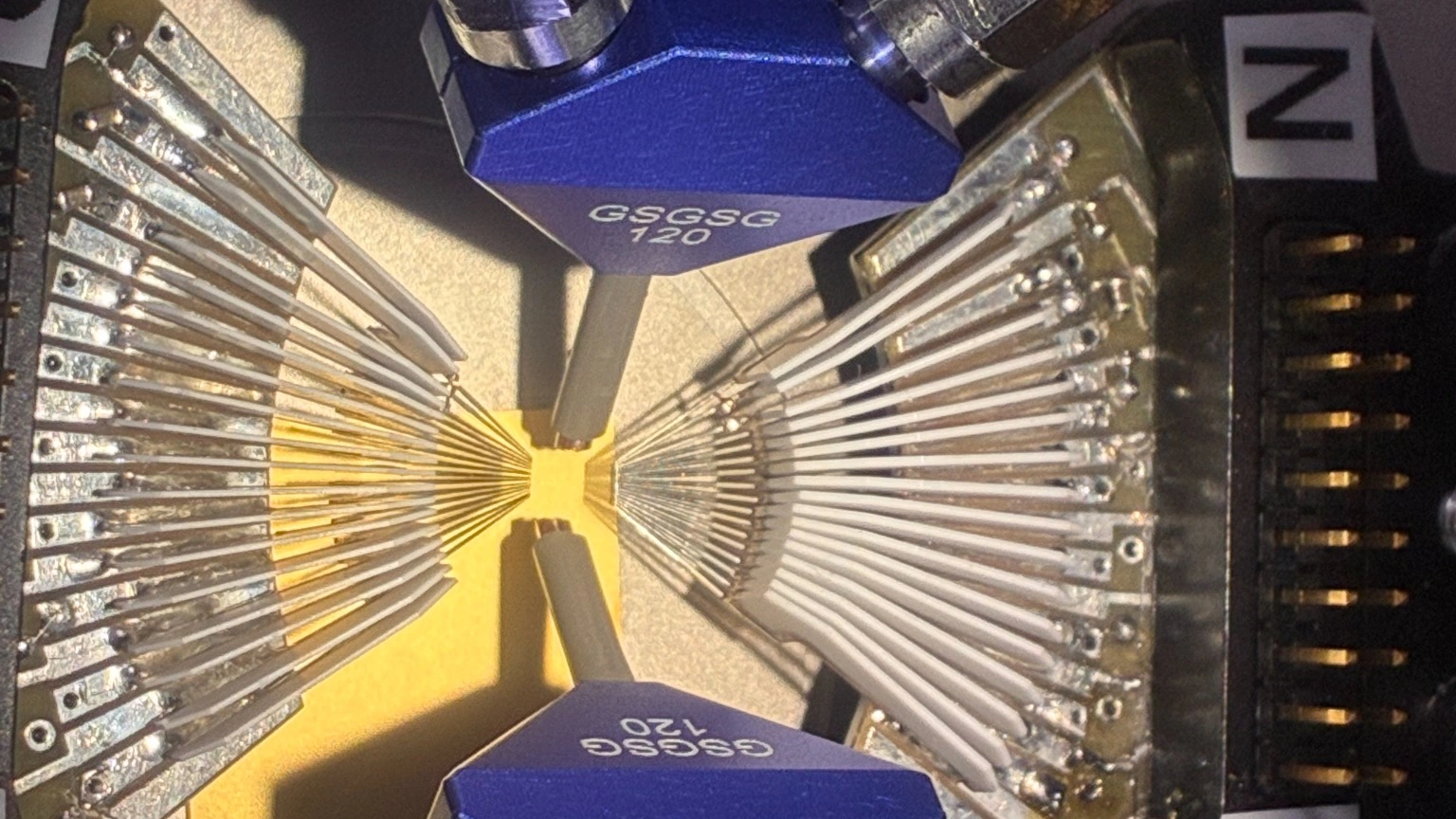
AI accelerators are pushing compute density, memory bandwidth and I/O bandwidth higher. But an RF probe does not measure an AI model, algorithm accuracy or processor throughput.
Its role is more specific: RF probing provides physical electrical access to the high-speed interfaces, interconnects and transitions that move data into, out of and between advanced computing devices.
As AI and high-performance computing architectures adopt higher-speed serial links, chiplets and denser packaging, the measurement problem is moving closer to the die while the electrical path between functional blocks becomes harder to characterize.
Faster computing creates a harder interconnect measurement problem. The important question for an RF or signal-integrity engineer is not whether a device is “for AI,” but where the critical electrical path is located and how it can be accessed without the measurement interface obscuring the DUT.
The industry direction is already visible. UCIe 3.0 supports 48 GT/s and 64 GT/s data rates for next-generation multi-chip systems, while OIF continues work on CEI-224G electrical interfaces spanning chip-to-module, chip-to-chip and longer electrical reaches.
Why AI Computing Is Making High-Speed Interconnects Harder to Measure
A modern AI computing platform is not simply a processor mounted on a PCB. Depending on the architecture, the electrical path may pass through compute dies, I/O chiplets, package substrates, interposers, high-speed SerDes interfaces, PCB launches, connectors, cables and the electrical interfaces surrounding optical engines.
System performance therefore depends not only on the silicon logic but also on the electrical quality of the paths carrying data between these elements.
For an RF or signal-integrity engineer, the practical questions are familiar:
- How much insertion loss is introduced by the channel?
- Where are the dominant reflections?
- Does impedance remain controlled through a package or PCB transition?
- Is a launch, connector or fixture creating a significant discontinuity?
- How does the channel behave in the frequency and time domains?
- Where should the measurement reference plane be established?
- Can the DUT be accessed without the probe or fixture becoming the dominant discontinuity?
RF probing is one way to obtain localized electrical access to these structures during characterization.
What Engineers Actually Measure
The phrase “AI accelerator testing” is broad. From an RF probing perspective, it is more useful to identify the actual electrical structures being measured.
High-Speed Differential I/O and SerDes
One of the clearest connections between AI computing and RF measurement is the high-speed serial interface. The measurement target is the electrical channel carrying the data—not the AI workload itself.
Depending on the development stage, engineers may characterize insertion loss, return loss, differential response, impedance discontinuities, mode conversion, package launches, PCB transitions and time-domain behavior.
OIF’s CEI-224G work includes very-short-reach chip-to-module and medium-reach chip-to-chip interfaces, illustrating how high-speed electrical links are moving through increasingly demanding physical channels.
RF probing can provide localized access during this type of interconnect characterization. Complete compliance or link validation, however, depends on the applicable standard, instrument set, fixtures, calibration and test methodology.
Die-to-Die and Chiplet Interconnects
Chiplet architectures change where engineers may need electrical access. Instead of treating the processor as one monolithic die, functions can be distributed among compute, I/O, memory-related and accelerator dies connected through high-speed die-to-die links.
From a measurement perspective, the relevant object is not the word chiplet itself. It is the electrical path between functional blocks.
Engineers may therefore need to evaluate channel loss, reflections, impedance continuity, interposer or substrate transitions, package escape structures and physical access to localized electrical nodes.
UCIe is one major industry effort addressing interoperable die-to-die connectivity. The current specification supports data rates up to 64 GT/s, which reinforces a broader measurement trend: high-speed electrical characterization is moving closer to the die and into increasingly dense package structures.
RF probing can support electrical characterization during chiplet development, but the probe itself is not a complete UCIe compliance solution.
Advanced Package Transitions
Advanced packaging changes both the electrical path and the possible measurement plane. A conventional path might be simplified as:
A more highly integrated architecture may involve multiple dies, interposers, redistribution structures or package substrates before the signal reaches the PCB. That creates useful measurement locations at wafer, bare-die, package, test-coupon and board level.
The important point is that the probe requirement changes with the measurement plane.
Package-to-PCB High-Speed Channels
Even when an accelerator die and package are electrically well designed, data still has to leave the package. The signal may encounter a package escape, PCB launch, transmission line, connector, module or cable before reaching the next electrical boundary.
Each transition becomes part of the channel. This is why high-speed computing measurement often extends beyond the semiconductor device into PCB traces, connectors, adapters and test interconnects.
Electrical Interfaces Around Photonics
AI infrastructure is also increasing demand for higher-bandwidth optical connectivity. From an RF probing perspective, the relevant boundary is the electrical side of the optical system.
Electrical interfaces remain around modulator drivers, photonic integrated circuits, optical engines and ASIC-to-optical-engine transitions. RF probing can therefore be relevant to electrical characterization at the boundary between high-speed electronic and photonic systems.
The probe is not measuring the optical signal itself.
Chiplets Move Measurement Closer to the Die
As integration becomes denser, electrical access can move from conventional board-level test points toward package and die-level structures.
This makes physical geometry a first-order engineering constraint. Pad dimensions, pitch, probe contact geometry, positioning accuracy and surrounding mechanical access can determine whether a measurement is practical before the VNA or TDR is even connected.
For fine-pitch wafer and die structures, smaller contact geometry and precise positioning become central. The AQUILA™ precision RF probe platform is positioned for microwave and mmWave wafer characterization, including small-pad access and 10 µm tip-radius configurations.
That is a different measurement problem from a populated PCB or production-oriented test environment.
Advanced Packaging Changes the Measurement Plane
It is more useful to classify probing by measurement plane and DUT geometry than by the end-market label alone.
| Measurement Plane | Typical Access Challenge | Probe Consideration |
|---|---|---|
| Wafer / fine-pitch die | Small pads, tight spacing, precise landing | Fine contact geometry and positioning control |
| Package / test coupon | Dense transitions and localized electrical nodes | Geometry matched to the available access structure |
| PCB / PCBA | Board transitions, surface tolerance, mechanical clearance and repeated touchdown | Robust contact architecture and practical board-level access |
For PCB and repeated-test environments, the LYRA™ ACP RF probe platform emphasizes high-durability probing and practical PCB contact. For wafer and fine-pad measurement, AQUILA is optimized around a different set of mechanical priorities.
An “AI probe” is therefore not a particularly useful technical category. Fine-pitch wafer probing, package-level electrical characterization and differential PCB probing are more meaningful descriptions.
What 224G-Class Interfaces Mean for RF and SI Measurement
Higher electrical lane rates reduce the margin available for uncontrolled discontinuities. The exact test methodology depends on the interface and applicable standard, but several familiar effects become more important as the electrical channel becomes more demanding:
- insertion loss and return loss,
- impedance control,
- connector and launch behavior,
- fixture contribution,
- calibration and reference-plane placement,
- and connection / landing repeatability.
OIF continues to develop CEI-224G electrical interfaces across multiple reach classes. At the test-equipment level, Keysight is also positioning 224 Gbps electrical and optical validation within next-generation 1.6T and AI data-center interconnect development.
For the measurement engineer, one consequence is especially important:
A poorly controlled probe landing, cable, adapter, connector or PCB transition can begin to obscure the behavior of the DUT itself.
This is why higher-speed measurement is not simply a question of choosing an instrument or probe with a larger bandwidth number. The path into the DUT must also be controlled.
Where RF Probing Fits into the Measurement Chain
A conventional connectorized test port is not always available at the electrical node an engineer needs to investigate. RF probing solves the physical-access problem by connecting a localized DUT structure into the wider measurement system.
The Vinstronics RF probe platform spans PCB- and wafer-oriented probing architectures for microwave and mmWave measurement. The appropriate architecture depends on DUT geometry, frequency range, pitch, contact topology and the intended measurement environment.
Probe selection therefore needs to consider both sides of the interface.
On the DUT side: contact topology, pitch, landing geometry, pad accessibility and mechanical clearance.
On the instrument side: required bandwidth, RF interface, cable performance, calibration, reference plane and measurement methodology.
Neither side can be evaluated in isolation.
The instrument-side path also deserves attention. RF coaxial cables and test interconnects need to support the intended bandwidth while maintaining practical routing and connection repeatability in the test setup.
Differential PCB Access Is a Different Problem from Wafer Probing
Board-level AI accelerator and high-speed computing hardware presents a different access problem from wafer or bare-die characterization.
At PCB level, engineers may need to access differential transmission structures without conventional coaxial connectors. If the DUT provides two accessible signal landing positions but no practical local ground pads at the probe landing area, an SS topology may be appropriate—provided that the DUT return-path structure and measurement objective are compatible with that topology.
For this decision, see SS vs. GSSG RF Probes for Differential PCB Testing.
Once the contact topology is selected, the physical relationship between the probe and PCB becomes the next problem. Probe pitch and PCB pad geometry should be reviewed together rather than treated as independent specifications.
Required bandwidth is another independent decision. A higher-frequency probe does not by itself create a higher-bandwidth measurement system; VNA capability, cable and adapter performance, calibration and the DUT transition all remain part of the chain. See 40 GHz vs. 67 GHz SS Differential RF Probes for the board-level bandwidth-selection logic.
The Electrical Side of Silicon Photonics and Co-Packaged Optics
AI infrastructure is increasing demand for higher-bandwidth optical connectivity, which creates another important electrical measurement boundary.
RF probes do not measure optical power, wavelength or optical modulation directly. Their role is on the electrical side of the electro-optic path, where engineers may need access to driver interfaces, photonic IC electrical pads, optical-engine interfaces or ASIC-to-optical-engine transitions.
For fine electrical pads on photonic and RFIC structures, a wafer-oriented architecture such as AQUILA™ is a more natural discussion point than a general PCB probe.
The technically useful description is therefore RF probing for the electrical side of silicon photonics and co-packaged optics, not simply “RF probes for optical testing.”
Beyond 224G: The Next Measurement Challenge
The industry is already examining electrical interfaces beyond 224G. OIF released a CEI-448G framework to define application spaces, technical challenges and potential solution paths for future 448 Gbps-per-lane interfaces.
The framework is a foundation for future implementation work rather than a mature mainstream compliance ecosystem today.
For measurement engineers, the direction matters more than the marketing number. As electrical rates continue to increase, access structures, transitions, calibration, fixture control and reference-plane definition become more—not less—important.
What RF Probes Do Not Measure
The term AI test can easily become too broad.
RF probes should not be presented as devices that directly determine AI model accuracy, GPU or NPU compute throughput, software performance, workload efficiency or complete protocol compliance.
Their value lies in a narrower but technically important role:
That may include high-speed I/O, chiplet development structures, package transitions, differential PCB channels and the electrical interfaces surrounding photonic systems.
Keeping this boundary clear makes the application case stronger, not weaker.
Faster Compute Means Harder Interconnect Measurement
AI computing is changing test and measurement because system performance increasingly depends on moving large amounts of data reliably across multiple physical interfaces.
RF probing provides access to selected electrical points within that path for frequency-domain and time-domain characterization. But the probe itself is only one part of the solution.
Probe geometry, DUT landing structure, interconnect bandwidth, test cables, calibration, reference plane and measurement repeatability have to be considered together.
For Vinstronics, the application direction is therefore broader than any single probe model: precision probing for wafer and die structures, durable probing for PCB and repeated-test environments, differential access for board-level channels, and precision RF interconnects connecting the DUT to the measurement instrument.
The opportunity is not simply “AI testing.”
FAQ
Do RF probes test AI algorithms or AI compute performance?
No. RF probes provide electrical access to high-speed hardware interfaces and interconnects. AI model accuracy and compute throughput are different test domains.
Where can RF probing be used in AI hardware development?
Depending on the DUT and measurement objective, RF probing may be relevant at wafer, die, package-test-structure or PCB level, as well as at electrical interfaces around photonic systems.
Is one probe architecture suitable for wafer, package and PCB measurement?
No. Contact geometry, pitch, mechanical access, surface condition and measurement plane can require different probe architectures. The DUT geometry should drive probe selection.
Can an RF probe by itself perform 224G or UCIe compliance testing?
No. The probe can provide electrical access during characterization, but complete compliance or link validation requires the applicable instruments, calibration, fixtures and test methodology.
Why does the complete RF path matter at higher data rates?
Because cable loss, adapters, probe transitions, fixture behavior, PCB launches and reference-plane placement can all contribute to the measured response. The probe bandwidth alone does not define the complete measurement system.
Need to Define the Right RF Probe Architecture?
Send the DUT type, landing geometry, required bandwidth and measurement plane. Vinstronics can review the appropriate probe and RF interconnect approach for your test setup.