In high-frequency PCB testing, the connector choice can affect more than how the cable attaches to the board. It can influence launch repeatability, rework risk, validation speed, board damage, fixture setup and how quickly an engineering team can move from prototype to test data.
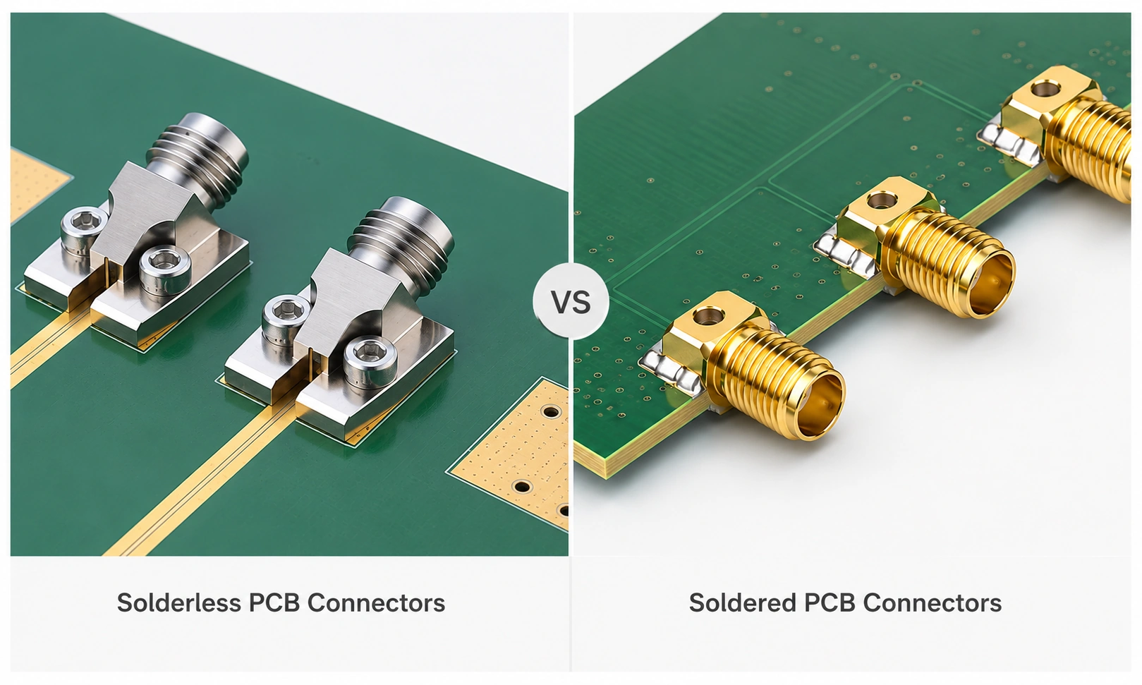
That is why solderless PCB connectors and soldered PCB connectors should not be compared only by installation method. They solve different problems in PCB development, RF validation and production hardware.
Engineer’s Selection Problem
The real question is not simply whether the connector should be soldered or screw-mounted. The better question is whether the PCB is in early validation, repeated testing, final production, fixture development or high-frequency launch debugging.
Short answer: Use solderless PCB connectors when fast installation, repeatable testing, board rework avoidance and prototype validation matter. Use soldered PCB connectors when the design is mature, the connector location is fixed and the assembly is intended for long-term production use. For high-frequency PCB testing, the best choice depends on frequency range, PCB stackup, launch geometry, test cycles and how much risk the team can accept during rework.
This article compares solderless and soldered PCB connectors from a high-frequency PCB testing perspective. For product-family information, review Vinstronics solderless PCB connectors and precision RF connectors.
Why PCB Connector Choice Matters at High Frequencies
At lower frequencies, connector installation may be treated as a mechanical or assembly detail. At microwave and mmWave frequencies, the connector launch becomes part of the RF path. Small changes in ground transition, pin position, solder quality, compression contact, board thickness or fixture alignment can affect the measured result.
For engineering teams, the connector decision often affects:
- How quickly a PCB can be tested after fabrication
- Whether the board can be reused after connector removal
- How much rework risk is acceptable
- Whether the test setup needs repeated connector installation
- Whether launch geometry must be changed during debugging
- Whether the connector will remain in the final product
This is why solderless and soldered PCB connectors should be selected according to the testing stage, not only the connector interface.
Quick Comparison Table
| Selection factor | Solderless PCB connector | Soldered PCB connector |
|---|---|---|
| Installation method | Usually compression or screw-mounted contact. | Soldered center pin and/or ground structure. |
| Best used for | Prototype validation, repeated testing, launch debugging and board reuse. | Mature designs, production assemblies and permanent board connections. |
| Rework risk | Lower board damage risk when installed and removed correctly. | Higher risk if repeated soldering, desoldering or rework is required. |
| Testing speed | Faster for engineering validation and connector changes. | Slower when soldering and inspection are required. |
| Main concern | Board thickness, compression force, screw pattern, launch geometry and repeatable mounting. | Solder quality, thermal process, footprint design, cleaning and final assembly reliability. |
When Solderless PCB Connectors Make More Sense
Solderless PCB connectors are often used when engineers need fast, repeatable access to high-frequency PCB test points without committing to a soldered interface. This is especially useful during early design validation, board bring-up and RF launch debugging.

They are commonly preferred when:
- The PCB is a prototype or validation board.
- The team needs to test multiple board revisions.
- The connector may need to be removed or repositioned.
- The board should not be exposed to soldering or desoldering cycles.
- The project requires fast RF measurement after board fabrication.
- The launch geometry may still be under evaluation.
- Repeated testing is required across several samples.
The value of a solderless connector is not only installation speed. It can also reduce rework risk and help engineering teams test high-frequency PCB paths before the final connector strategy is locked.
Engineering note: Solderless does not mean careless installation. Board thickness, mounting torque, ground contact, compression geometry and launch design still need to be controlled.
When Soldered PCB Connectors Are Still the Better Choice
Soldered PCB connectors remain important for mature designs and production hardware. When the footprint is validated, the launch structure is fixed and the connector will remain on the board, soldered connectors can provide a permanent and compact interface.
They are usually a better fit when:
- The design is already validated.
- The connector location will not change.
- The board is intended for final production or long-term use.
- The assembly process is controlled and repeatable.
- The project does not require repeated connector removal.
- The footprint and launch geometry have already been tuned.
The tradeoff is rework risk. If a soldered connector must be removed several times during PCB debugging, the board pad, launch area or ground structure can be damaged. That risk is one reason engineering teams often use solderless connectors during early test stages and move toward soldered connectors once the design is stable.

Solderless Connectors in High-Frequency PCB Testing
High-frequency PCB testing often requires engineers to separate two questions:
- Is the board design performing as expected?
- Is the connector launch or assembly process affecting the measurement?
A solderless connector can help during validation because it reduces the variables created by soldering, rework and thermal exposure. It also allows the team to test multiple PCB samples or revisions more efficiently.
Typical use cases include:
- 2.92mm PCB launch validation
- 2.4mm high-frequency PCB testing
- 1.85mm precision board-level test setups
- High-speed digital and RF transition evaluation
- Microwave PCB prototype bring-up
- Fixture-based board testing
- Engineering sample validation before production release
For high-frequency connector family review, see Vinstronics 2.92mm RF connectors, 2.4mm RF connectors and 1.85mm RF connectors.
Connector Launch and PCB Stackup Matter
Whether the connector is solderless or soldered, the PCB launch must be designed for the target frequency range. The connector alone cannot compensate for an unsuitable transition.
Key PCB details include:
- Board thickness
- Dielectric material
- Transmission line type
- Ground via pattern
- Pad geometry
- Launch transition
- Connector mounting area
- Available clearance around the connector
For solderless connectors, board thickness and compression contact are especially important. For soldered connectors, footprint design and solder quality become critical. In both cases, the launch should be evaluated as part of the RF path.
Selection by Development Stage
| Project stage | Better connector direction | Why |
|---|---|---|
| Early PCB prototype | Solderless PCB connector | Supports fast test access and reduces rework risk. |
| Launch debugging | Solderless PCB connector | Allows repeated evaluation across board revisions. |
| Fixture-based RF testing | Solderless or replaceable connector | Improves serviceability and setup flexibility. |
| Design validation complete | Soldered PCB connector | Suitable when the connector location and launch structure are final. |
| Production hardware | Soldered PCB connector | Works well when the assembly process is controlled and repeatable. |
When You May Need Both
Some engineering programs use both connector types at different stages. A solderless connector may be used for prototype validation and launch debugging, while a soldered connector may be selected later for production hardware.
This is often a practical workflow:
- Use solderless connectors to test the PCB path quickly.
- Compare board revisions without repeated soldering.
- Validate the launch geometry and frequency performance.
- Move to soldered connectors if the final product needs a permanent interface.
The important point is to treat connector choice as part of the development process, not as a one-time catalog selection.
Common Selection Mistakes
| Mistake | Why it matters | Better approach |
|---|---|---|
| Choosing only by connector interface | A 2.92mm or 2.4mm connector still needs a suitable launch structure. | Review connector, PCB stackup and launch geometry together. |
| Using soldered connectors too early | Repeated rework can damage pads or change the launch area. | Use solderless connectors during early validation when board changes are likely. |
| Treating solderless mounting as universal | Board thickness, compression geometry and screw pattern must fit the connector design. | Check mechanical compatibility before layout or ordering. |
| Ignoring test repeatability | Connector installation variation can affect measurement results. | Control mounting method, torque, ground contact and calibration setup. |
What to Provide for Connector Review
For high-frequency PCB connector review, useful information includes both electrical and mechanical details.
- Target frequency range
- Connector family: SMA, 2.92mm, 2.4mm, 1.85mm or others
- PCB thickness and material
- Transmission line type
- Launch geometry or layout screenshot
- Ground via pattern
- Available board space around the connector
- Prototype or production stage
- Expected number of test cycles
- Whether the connector must be removed or reused
If the connector will be used with external test cables, also review the related RF Cable Assemblies Guide and the custom RF cable assembly specification checklist.
How Vinstronics Reviews Solderless and Soldered PCB Connector Requirements
Vinstronics reviews PCB connector requirements based on frequency range, connector interface, board thickness, launch design, installation method, test stage and expected use condition.
For early high-frequency PCB testing, solderless PCB connectors can help reduce rework risk and speed up validation. For mature production hardware, soldered PCB connectors may be more suitable when the footprint and process are already controlled.
Related product areas include Vinstronics solderless PCB connectors, precision RF connectors and RF cable assemblies.
FAQ
What is the main difference between solderless and soldered PCB connectors?
Solderless PCB connectors use a mechanical or compression-style installation method, while soldered PCB connectors are attached through soldering. The better choice depends on PCB test stage, frequency range, rework risk and production requirements.
When should I use solderless PCB connectors?
Use solderless PCB connectors for prototype validation, high-frequency PCB testing, launch debugging, repeated board evaluation and situations where board rework risk should be reduced.
When are soldered PCB connectors better?
Soldered PCB connectors are usually better for mature designs, production assemblies and permanent board connections where the footprint, launch structure and assembly process are already controlled.
Are solderless PCB connectors suitable for high-frequency testing?
Yes, when the connector design, board thickness, launch geometry and mounting method are matched correctly. The complete PCB transition should still be reviewed for the target frequency range.
What information is needed to select a PCB connector?
Useful information includes target frequency, connector family, PCB thickness, board material, launch geometry, ground via pattern, available space, test stage and whether the connector must be removable.
Need help selecting a PCB connector for high-frequency testing?
Send your target frequency, PCB thickness, launch geometry, connector interface and test stage. Vinstronics can review whether a solderless or soldered PCB connector approach is more suitable.