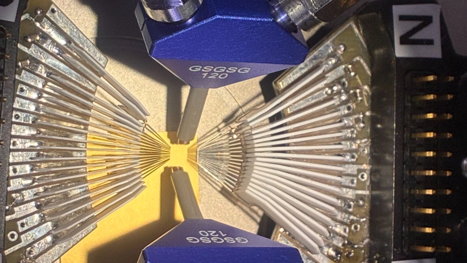
A PCB may be designed for high-speed differential measurement and still be difficult to probe if the layout does not provide local ground pads. In this case, the probing method becomes part of the measurement problem — not just the final accessory connected to the VNA.
For high-frequency PCB and PCBA validation, the test point is not always arranged as an ideal GSG or GSSG pad structure. Dense routing, limited board space, package keep-out areas, solder mask openings, and prototype constraints can all make local grounding difficult.
For suitable differential structures, an SS RF probe can provide a practical signal-to-signal probing method. Instead of requiring a ground contact at the probe landing area, an SS probe contacts the two signal pads directly and supports differential S-parameter measurement at the board level.
An SS RF probe can be useful when a differential PCB structure does not provide nearby ground pads. The final measurement quality still depends on pad pitch, signal geometry, return-path behavior, probe-tip calibration, cable stability, fixture rigidity, and touchdown repeatability.
The Vinstronics VST-D67G-SS-XXX series is designed for DC–67 GHz SS differential probing with pitch options selected according to the DUT pad layout. It is intended for engineers who need direct PCB-level differential measurement where local ground pads may be limited or unavailable.
For a broader overview of available probe formats, see Vinstronics RF probe solutions. For available signal-to-signal models, view the Vinstronics SS Probe series.
Why Local Ground Pads Become a Problem
Many high-frequency test structures are designed with dedicated probe pads. In that case, a GSG, GSSG, or GSGSG probe can be selected according to the pad pattern. But real engineering boards are not always so convenient.
During prototype validation, failure analysis, or compact module testing, engineers may encounter differential traces without a nearby ground landing area. Adding temporary ground wires, scraping solder mask, or modifying the PCB can change the test condition and slow down the measurement workflow.
Common PCB-Level Test Constraints
- Differential pads without nearby ground pads
- Limited landing area around high-density routing
- Prototype boards not designed for connector launches
- Package or component clearance near the test point
- Fixture access limits in automated test setups
- Need for repeated, non-destructive board-level probing
An SS probe does not automatically solve every return-path or layout problem. However, when the DUT is a suitable differential structure and the measurement setup is controlled, SS probing can reduce dependence on local ground-pad geometry.
What an SS RF Probe Actually Solves
An SS probe uses a signal-signal contact pattern. For suitable differential PCB structures, this allows direct contact to the two signal pads without a dedicated ground needle at the same landing area.
This is especially useful when the engineer wants to evaluate a differential structure directly on the PCB, rather than adding a connector, soldering temporary cables, or redesigning a test coupon only to create a probing interface.
SS Probing Is Most Useful When
- The DUT is a differential PCB or PCBA structure
- The available landing pads are signal-to-signal
- Local ground pads are limited or unavailable
- The test objective is differential S-parameter measurement
- The probe pitch can be matched to the pad layout
- The calibration and de-embedding method are defined
When SS Probing May Not Be the Right Choice
SS probing should not be treated as a universal replacement for GSG or GSSG probing. If the DUT requires a clearly defined ground reference at the probe landing point, or if the layout already provides a controlled GSG / GSSG pad structure, another probe configuration may be more appropriate.
Engineering Boundary
SS probing can simplify differential contact when local ground pads are limited, but it does not remove the need to evaluate the return path, calibration plane, fixture stability, and DUT layout. The probe must match the measurement structure, not only the target frequency.
For single-ended RF paths, grounded coplanar structures, or DUTs designed specifically for GSG / GSSG probing, the correct choice may still be a GS, SG, GSG, or GSSG probe.
SS vs GSG vs GSSG: How to Choose
| DUT Pad Layout | Probe Direction | Engineering Note |
| S-S | Consider SS | Useful for suitable differential structures where local ground pads are limited or unavailable. |
| G-S-G | Use GSG | Common for single-ended RF or grounded coplanar structures. |
| G-S-S-G | Use GSSG | Common for differential structures with dedicated ground pads on both sides. |
| Non-standard layout | Request review | Pad pitch, approach angle, and calibration method should be reviewed before selecting the probe. |
The most important rule is simple: start with the DUT pad layout, then select the probe. A 67 GHz probe can still be the wrong probe if the contact pattern or pitch does not match the board.
If your DUT uses grounded pad layouts, compare Vinstronics GS / SG probes, GSG probes, and GSSG / GSGSG probes before selecting an SS configuration.
67 GHz Measurement Setup Considerations
At frequencies up to 67 GHz, the probe is only one part of the measurement chain. The VNA, RF cables, adapters, probe station, calibration substrate, board fixture, and DUT pad design all affect the measured result.
For this reason, SS probe selection should be reviewed as part of the complete RF path.

Measurement Setup Checklist
- Probe pitch matched to the PCB pad layout
- Stable probe station or positioner setup
- Low-loss RF cable path with controlled bending
- Compatible 1.85 mm interface and adapter path
- Calibration at or near the probe tip
- Clean probe tips and clean PCB landing pads
- Repeatable touchdown force and alignment
For the rest of the test chain, engineers may also need suitable RF cable assemblies, adapters, calibration substrates, and probe station accessories.
VST-D67G-SS-XXX Series: Key Configuration
The Vinstronics VST-D67G-SS-XXX series is designed for DC–67 GHz differential probing using an SS tip configuration. The series supports pitch selection according to the actual PCB pad layout.
For the 67 GHz configurable-pitch version, see the VST-D67G-SS-XXX 67 GHz SS RF probe. For applications up to 40 GHz using 2.92 mm female interfaces, the VST-D40G-SS-XXX 40 GHz SS RF probe may be a suitable option.

| Parameter | VST-D67G-SS-XXX Series |
| Frequency range | DC–67 GHz |
| Tip configuration | SS signal-to-signal |
| Impedance | 100 Ω differential |
| RF interface | 1.85 mm Female |
| Connector angle | 45-degree |
| Pitch range | 350 µm–3000 µm |
| Standard pitch step | 120 µm |
| Contact force | 5 g |
The 45-degree connector layout helps keep the RF cable path practical in probe stations and automated test setups, especially when multiple probes, fixtures, or microscope access are involved.
Example Configuration: VST-D67G-SS-800
The model number VST-D67G-SS-800 represents a DC–67 GHz SS probe with an 800 µm signal-to-signal pitch. This configuration can be used as an example of how the series is specified for a defined PCB pad pitch.
Reference Data Note
Typical SDD11 and SDD21 electrical characteristics are available for the 800 µm pitch reference configuration. Performance for other pitch options should be reviewed according to the actual probe configuration, DUT layout, calibration method, and test setup.
This distinction is important. The 800 µm version provides a useful reference, but the full VST-D67G-SS-XXX series should be selected according to the actual pad pitch and board-level measurement environment.
Ordering Logic: What “XXX” Means
In the model name VST-D67G-SS-XXX, the final three digits indicate the required pad pitch in microns.
Model Format
VST-D67G-SS-XXX
- D67G = DC–67 GHz differential probe series
- SS = signal-to-signal tip configuration
- XXX = pad pitch in microns
Example: VST-D67G-SS-800 refers to a DC–67 GHz SS probe with 800 µm pitch.
What to Send for Probe Selection Review
To recommend the correct SS probe configuration, the actual DUT layout is more useful than the target frequency alone. Before requesting a quote or custom configuration, send the measurement conditions whenever possible.
Send These Details
- PCB pad pitch, preferably center-to-center
- Close-up board photo or pad layout drawing
- DUT type: PCB, PCBA, package coupon, module, or validation board
- Target frequency range and measurement objective
- Available probe station or positioner setup
- Required cable and adapter path
- Calibration substrate or calibration method
- Whether SDD11 / SDD21 reference data is required
This helps avoid a common selection problem: choosing a high-frequency probe that does not fit the actual board-level contact geometry.
Handling Notes for Repeatable Measurement
High-frequency probing depends on contact quality and setup repeatability. Even a suitable probe can produce poor data if the tips are contaminated, the cable path is unstable, or the calibration plane is not controlled.
Practical Handling Guidelines
- Perform calibration at the probe tip for best accuracy
- Avoid excessive force to preserve tip alignment
- Keep contact surfaces clean to maintain low contact resistance
- Store probes in protective cases when not in use
Conclusion
SS RF probes can be a practical option for PCB-level differential testing when local ground pads are limited or unavailable. They are especially useful when the DUT provides a signal-to-signal differential landing structure and the measurement setup is designed around probe pitch, calibration, cable stability, and fixture repeatability.
The Vinstronics VST-D67G-SS-XXX series supports DC–67 GHz SS differential probing with pitch options for different PCB pad layouts. For engineers working on high-speed interconnects, SerDes validation boards, mmWave differential circuits, and automated high-frequency PCB test setups, the correct probe selection should start from the DUT layout — not only the frequency rating.
Start with the DUT pad layout, then select the probe configuration, pitch, cable path, and calibration method.
FAQ
What is an SS RF probe?
An SS RF probe uses a signal-to-signal tip configuration. It is mainly used for suitable differential structures where the two signal pads can be contacted directly.
When should I consider an SS probe instead of GSG or GSSG?
Consider an SS probe when the DUT is a differential structure and nearby ground pads are limited or unavailable. If the DUT already provides GSG or GSSG pads, those configurations may still be more appropriate.
Does SS probing eliminate the need for calibration?
No. Calibration remains important. For high-frequency measurement, calibration should be performed at or near the probe tip whenever possible.
What does XXX mean in VST-D67G-SS-XXX?
XXX indicates the pad pitch in microns. For example, VST-D67G-SS-800 represents an SS probe with 800 µm pitch.
Is the 800 µm pitch data valid for every pitch option?
No. The 800 µm version should be treated as a reference configuration. Other pitch options should be reviewed according to the actual probe configuration and test setup.
Need Help Selecting an SS RF Probe?
Send your PCB pad layout, pitch, target frequency, probe station setup, and calibration method. Vinstronics engineers can help review the suitable SS probe configuration for your measurement setup.