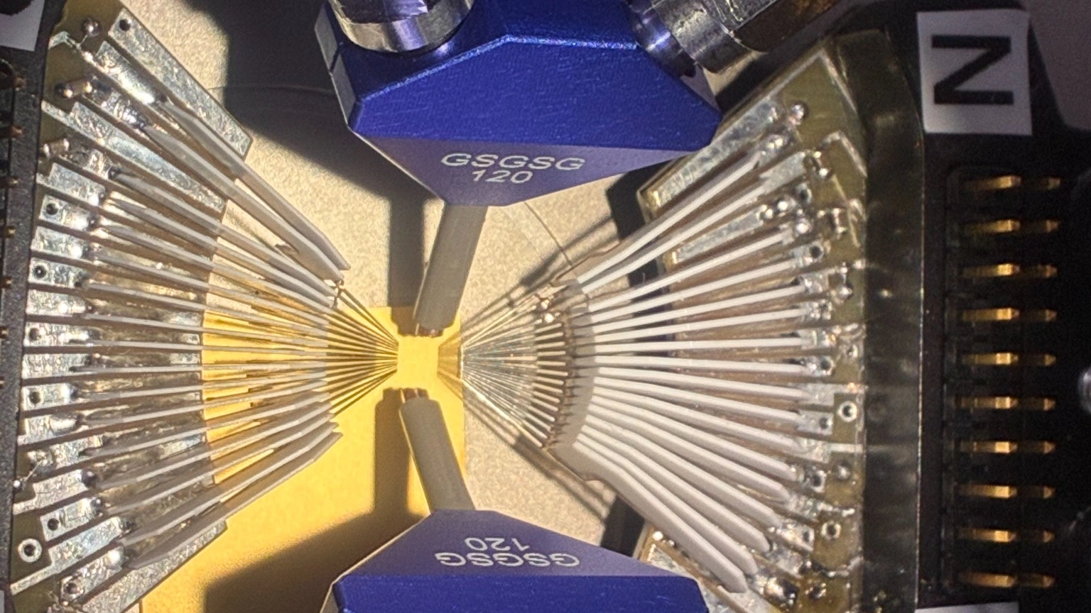
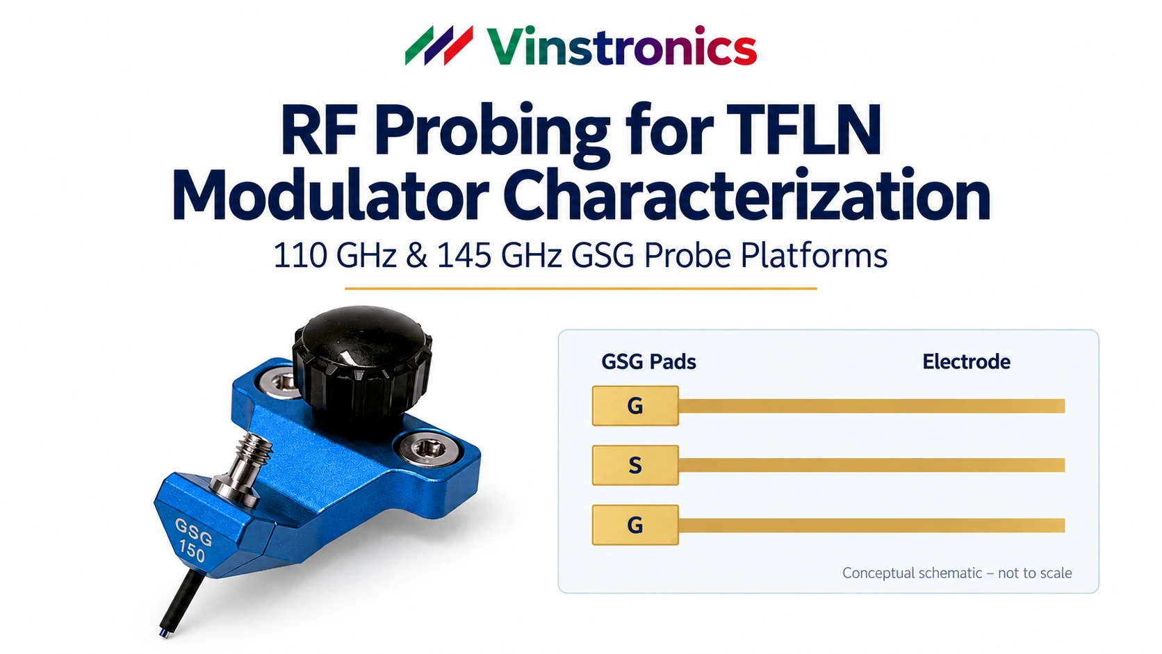
Extending an on-wafer measurement from 110 GHz to 145 GHz changes more than the upper frequency limit. At D-band, the probe transition, tip geometry, DUT pad layout, contact condition, calibration reference plane, and de-embedding all become material contributors to the measured response.
Vinstronics has introduced a family of DC–145 GHz RF probes for single-ended and differential device characterization. The platform combines 0.8 mm RF interfaces, specified 50 ±1 Ω and 100 ±2 Ω impedance control, configurable probe pitch, measured performance through 145 GHz, and S-parameter support for de-embedding workflows.
Why 145 GHz RF Probing Matters
D-band, commonly defined as 110–170 GHz, is an active research region for sub-terahertz communications, high-frequency semiconductor development, sensing, radar, advanced packaging, and broadband device characterization. Early 6G research is also exploring D-band as engineers evaluate wider channel bandwidths, RF front-end performance, and new sub-THz spectrum.
For device engineers, the practical challenge is not only generating or receiving a D-band signal. The measurement system still needs a controlled transition from the coaxial test path to microscopic pads on a wafer, package, test coupon, or other planar DUT. The RF probe provides that final electrical interface.
At 145 GHz, the probe is part of the RF transmission path—not just a mechanical contact.
Why Moving from 110 GHz to 145 GHz Is More Demanding
Shorter Wavelength Increases Sensitivity to Geometry
The free-space wavelength at 145 GHz is approximately 2.07 mm. As physical dimensions become a larger fraction of the wavelength, discontinuities in the connector transition, transmission structure, probe tip, and DUT pad geometry have a greater influence on impedance and reflection.
Impedance Continuity Becomes More Critical
A probe carries the signal through several different physical regions before it reaches the DUT. Maintaining controlled impedance through those transitions becomes increasingly important at D-band. The Vinstronics 145 GHz platform is specified at 50 ±1 Ω for single-ended GSG probes and 100 ±2 Ω for differential GSSG and GSGSG probes.
The Loss and Reflection Budget Tightens
Conductor loss, transition loss, radiation, contact condition, and mismatch all become more significant as frequency increases. The Vinstronics 145 GHz probe platform is specified at insertion loss <3.5 dB and return loss >10 dB through 145 GHz.
The Coaxial Interface Must Support D-Band Operation
The probe family uses a 0.8 mm female RF interface. This interface supports precision coaxial connectivity for measurements extending to 145 GHz while keeping the transition compact enough for probe-station integration.
What the Probe Must Solve in a 145 GHz Measurement Path
1. Provide the Final Controlled Interface to the DUT
High-frequency instrumentation does not directly contact wafer-level or planar device pads. The probe provides the transition from the coaxial measurement path to the DUT contact geometry, enabling direct S-parameter characterization of compatible devices and test structures.
2. Characterize the Probe Contribution to the Measurement
At D-band, the probe itself has measurable transmission loss and reflection. Its electrical behavior therefore needs to be characterized rather than treated as an ideal connection. Calibration establishes the measurement reference plane, while probe S-parameter data can support de-embedding of the probe contribution from the measured DUT response.
3. Match the Probe to the Actual Pad Layout
Different wafers, packages, test coupons, and interconnect structures use different pad dimensions and spacing. Vinstronics 145 GHz probes support a 100–1250 μm configurable pitch range, with 25 μm steps from 100–250 μm and 50 μm steps from 300–1250 μm.
Engineering principle: the probe pitch should follow the actual DUT pad geometry rather than forcing the DUT layout to fit one fixed probe pitch.
4. Support Single-Ended and Differential Topologies
The platform includes a 50 Ω GSG configuration for single-ended measurements and 100 Ω GSSG / GSGSG configurations for differential and mixed-mode characterization. The appropriate contact architecture should be selected from the DUT pad topology and measurement mode.
Vinstronics 145 GHz RF Probe Platform
| Frequency Range | DC–145 GHz — D-band measurement coverage |
|---|---|
| Single-Ended Impedance | 50 ±1 Ω — Single-ended GSG impedance |
| Differential Impedance | 100 ±2 Ω — Differential GSSG / GSGSG impedance |
| Insertion Loss | <3.5 dB — Specified insertion loss to 145 GHz |
| Return Loss | >10 dB — Specified return loss to 145 GHz |
| Configurable Pitch | 100–1250 μm — Configurable probe pitch |
All three probe architectures use a 0.8 mm female RF interface. Probe characterization files are available in S2P format for single-ended configurations and S4P format for differential / multi-port configurations to support de-embedding and mixed-mode analysis.
Representative Measured Performance to 145 GHz
Representative production test data from two VST-145G-GSGSG-100 probes show the measured differential response through 145 GHz. Both samples use a 100 μm pitch and a 0.8 mm interface.
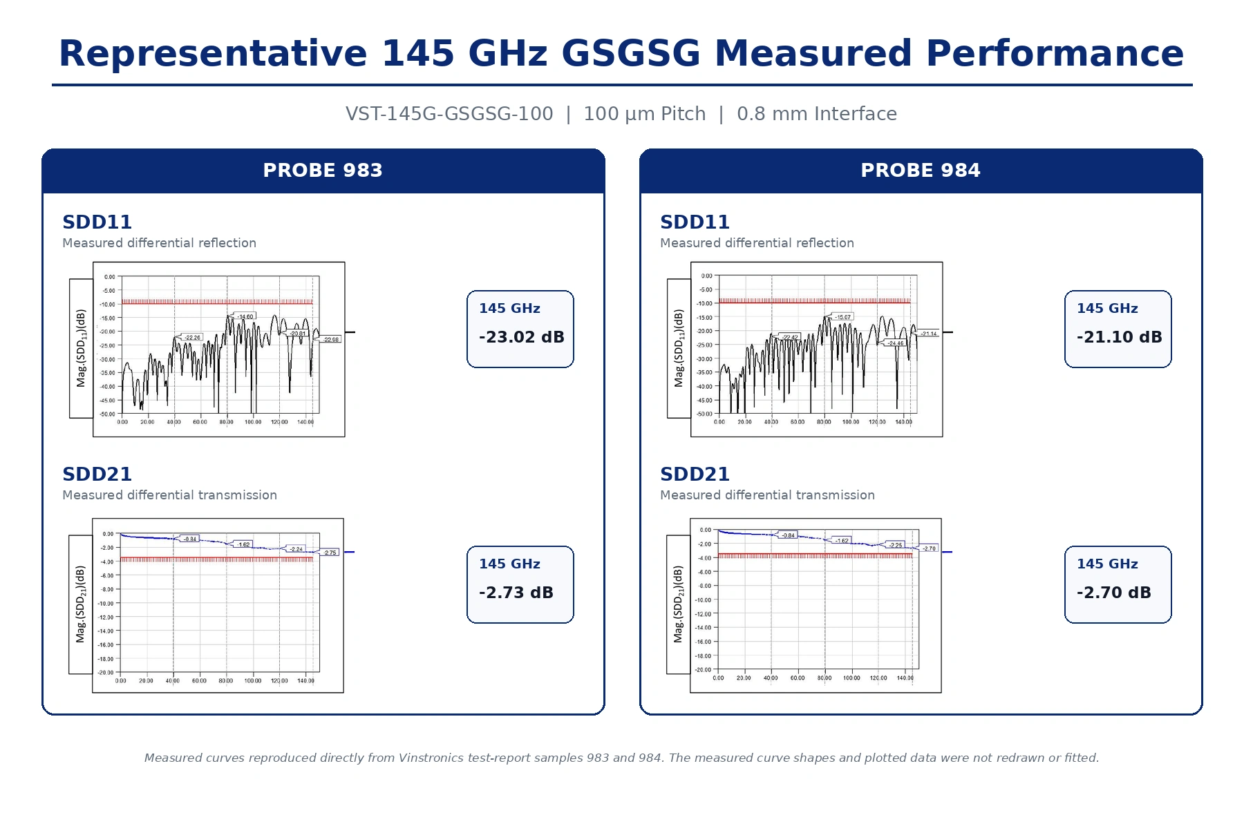
At 145 GHz, sample 983 measured SDD21 = -2.73 dB and SDD11 = -23.02 dB; sample 984 measured SDD21 = -2.70 dB and SDD11 = -21.10 dB. These are representative measured values from the two reported samples, not guaranteed endpoint values for every unit.
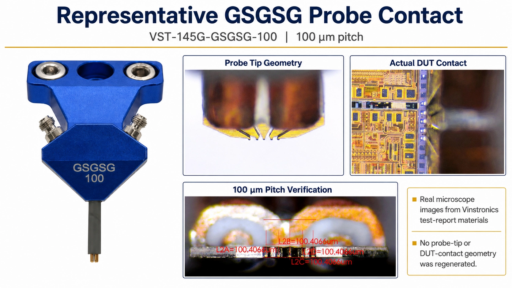
The test report also documents the real probe-tip geometry, 100 μm pitch verification, DUT contact condition, calibration structures, and the complete measured frequency sweep.
Current and Emerging Application Areas
D-Band and Early 6G Research
D-band is being investigated for future sub-terahertz communication research, wideband channel studies, RF front-end development, and experimental high-data-rate systems. On-wafer probing enables direct characterization of devices and test structures before they are integrated into a complete radio or module.
RFIC and MMIC Characterization
Amplifiers, mixers, multipliers, detectors, passive structures, and transceiver-related devices require measurement of gain, loss, matching, isolation, or differential behavior at the device level. A probe with measured performance through 145 GHz extends this characterization into D-band.
Radar, Sensing, and Imaging Research
D-band probing supports component and test-structure characterization for high-frequency radar, sensing, and imaging research where device behavior must be evaluated above conventional millimeter-wave bands.
Advanced Packaging and Interconnect Characterization
At higher frequencies, package transitions, transmission lines, chip-to-package interfaces, test coupons, and other interconnect structures can become a significant part of the measured channel response. Single-ended and differential probes allow these structures to be characterized directly with the contact geometry matched to the pad layout.
High-Speed Differential Interconnect Research
As electrical interfaces move toward higher symbol rates and broader characterization bandwidths, differential probing can be used to evaluate transmission lines, launches, packages, and test structures whose electrical behavior extends into the millimeter-wave region.
What to Evaluate Beyond the Frequency Rating
For D-band measurements, maximum frequency should not be evaluated in isolation. Engineers should consider the complete probe-to-DUT interface:
- Probe topology: single-ended or differential
- Impedance: 50 Ω or 100 Ω differential
- Insertion loss and return loss: across the required measurement band
- Pitch and pad geometry: matched to the DUT layout
- Coaxial interface: appropriate for the required frequency range
- Calibration reference plane: established for the selected probe and calibration method
- S-parameter characterization: available for de-embedding when required
- Contact condition: alignment, touchdown, pad condition, and contact repeatability
At 145 GHz, electrical transition design, mechanical geometry, calibration, and DUT pad structure need to be treated as parts of one measurement system rather than as independent details.
The Vinstronics 145 GHz Probe Family
The current Vinstronics 145 GHz family covers both single-ended and differential probing with three contact architectures for different DUT pad topologies.
| Model | Architecture | Typical Fit | Product |
|---|---|---|---|
| VST-145G-GSG-XXX | 50 Ω | G-S-G | Single-Ended | For compatible single-ended RF and millimeter-wave pad structures. | View 145 GHz GSG Probe |
| VST-145G-GSSG-XXX | 100 Ω | G-S-S-G | Differential | For differential layouts with adjacent signal pads and outer grounds. | View 145 GHz GSSG Probe |
| VST-145G-GSGSG-XXX | 100 Ω | G-S-G-S-G | Differential | For differential layouts that include an interleaved center ground. | View 145 GHz GSGSG Probe |
Planning a 145 GHz Probe Measurement?
Share your DUT pad layout, required pitch, signal configuration, measurement frequency, and probe-station setup. Vinstronics can review the probe configuration for your measurement application.