One of the practical advantages of a solderless vertical launch connector is that it can be removed and replaced without subjecting the PCB to another soldering process. That can simplify fixture development, PCB rework, connector replacement, and repeated access to the DUT.
But removability and measurement repeatability are not the same thing.
Each time a compression-mounted connector is removed and reinstalled, the mechanical boundary conditions of the RF launch are recreated. Connector seating, alignment, mounting condition, PCB flatness, contact-surface condition, cable loading, and the installation procedure can all influence the assembled transition.
For a high-frequency fixture, the useful question is therefore not simply:
Can the connector be removed and installed again?
It is:
Can the interface be recreated consistently enough to meet the measurement repeatability required by the application?
That distinction becomes increasingly important as measurement bandwidth increases and the connector-to-PCB transition becomes more sensitive to small mechanical changes.
For a broader discussion of how vertical RF access is used in high-speed validation fixtures, see
Vertical Launch Connectors for 112G / 224G SerDes Test Fixtures
.
What Repeatability Actually Means
Repeatability should be defined before it is evaluated.
For this discussion, reinstallation repeatability means comparing measurements made before and after removing and reinstalling the same connector under controlled conditions.
That is different from connector-to-connector reproducibility, where different connector samples are compared, or fixture-to-fixture reproducibility, where different boards or complete fixtures are compared.
Keeping those questions separate matters. Otherwise, connector variation, PCB variation, cable movement, calibration drift, and installation variation can all become mixed into a single result.
Install → Measure → Remove → Reinstall → Measure Again → Compare
The metrics being compared may include return loss, insertion loss, phase, resonance location, or other parameters important to the fixture.
The result belongs to the installed measurement system, not to the connector body alone.
Mounting Force Should Be Controlled, Not Maximized
A solderless vertical launch connector relies on mechanical installation to establish the intended signal and ground interface with the PCB.
The goal is not to apply as much force as possible. The goal is to reproduce the mounting condition for which the connector and PCB launch were designed.
Too little compression may prevent the interface from seating as intended. Too much can introduce unnecessary mechanical stress and, depending on the PCB construction, may contribute to local board deformation or warpage.
That distinction matters because mechanical deformation can change the geometry of the RF transition itself.
The appropriate mounting torque or force is therefore product-specific. It depends on connector construction, mounting hardware, PCB material and thickness, and the mechanical design around the launch.
A torque value used for one connector family should not be copied to another simply because both are compression mounted.
For Vinstronics products, any numerical mounting specification should come from the applicable product drawing or validated installation instruction.
Controlled installation is more important than maximum compression.
Alignment Is Part of the RF Transition
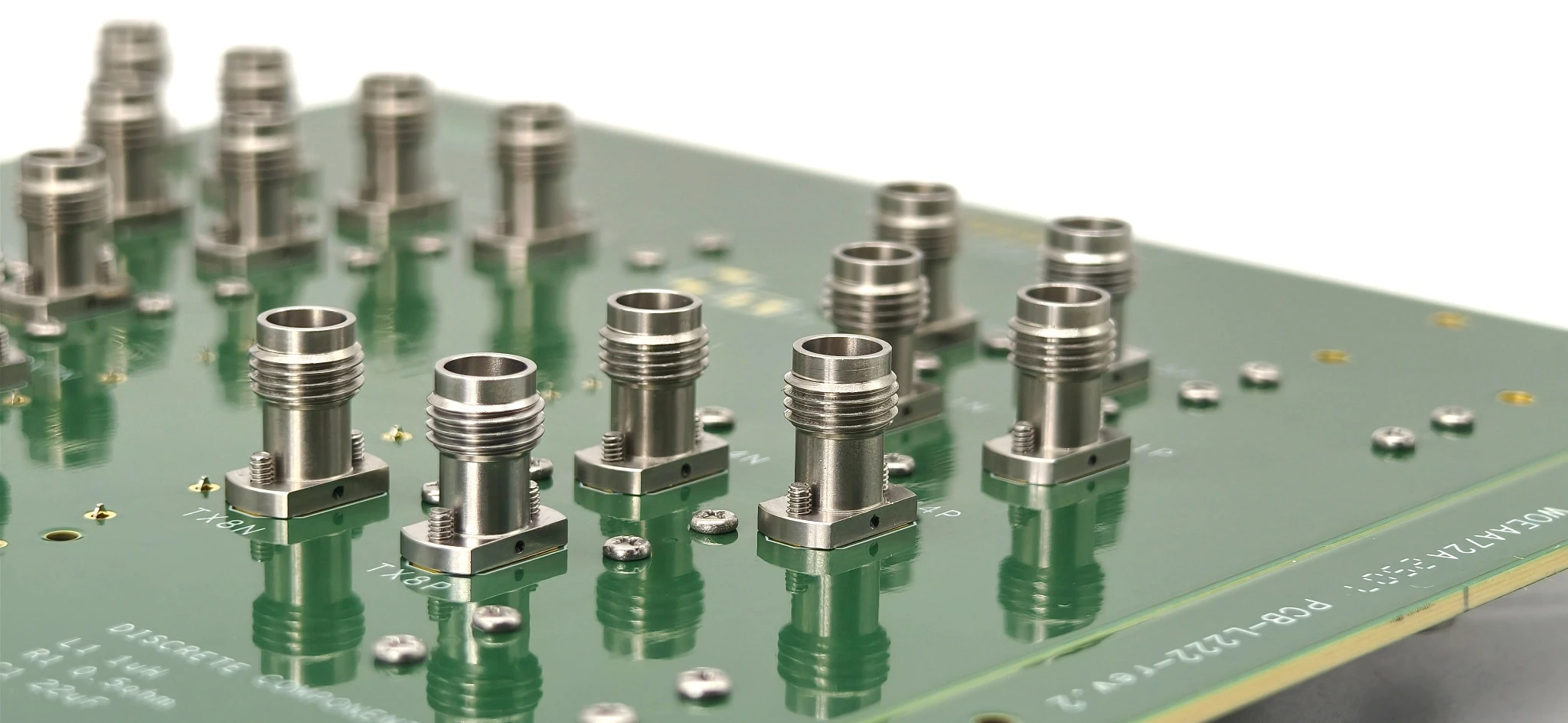
Mechanical alignment is also an electrical issue.
The signal contact must land where the PCB launch was designed to receive it, and the connector ground structure must engage the board in the intended geometry.
If the connector moves laterally, rotates, tilts, or seats unevenly, the assembled transition changes.
At sufficiently high frequencies, small offsets can alter the relationship between the signal contact, landing pad, surrounding ground structure, and transmission line. What appears to be a mechanical positioning error can therefore become an impedance discontinuity.
This also means alignment should be considered during the entire assembly process—not only when the connector is first placed on the board.
Attaching a threaded cable can apply torque to the board-mounted connector. Cable routing can introduce side load. Fastener tightening can shift the connector slightly before final seating.
Where the connector design requires anti-rotation or a particular fastening sequence, those instructions become part of the repeatable RF assembly process.
As discussed in
How PCB Launch Geometry, Ground Vias, and Return Path Affect Vertical Launch Connector Performance
,
the connector, PCB landing structure, ground return, and transmission line function as one RF transition.
Mechanical reinstallation recreates that transition.
The PCB Is Part of the Reusable Interface
The connector is only one of the two contact surfaces involved.
The PCB landing region should also be considered when a solderless connector is removed and reinstalled.
Contamination, debris, visible damage, abnormal contact marks, or changes in PCB flatness may alter how the connector seats. The significance of those changes depends on the connector contact design, PCB finish, bandwidth, and the fixture’s acceptance criteria.
This is why “field replaceable” should not be interpreted as “unlimited reuse.”
Unless a connector has a validated removal-and-reinstallation cycle specification, assigning an arbitrary number of reuse cycles would be misleading.
A more defensible approach is to inspect the interface and validate performance against the requirements of the actual measurement system.
Board support matters for the same reason. If the PCB bends differently from one installation to the next, the connector-to-board geometry is no longer being recreated under the same conditions.
Why the Measurement Can Change After Reinstallation
Suppose the fixture is measured, one connector is removed, and the next measurement changes after it is reinstalled.
That does not automatically mean the connector is defective.
The difference may come from connector seating, contact alignment, PCB surface condition, board deflection, mounting hardware, cable movement, or a change elsewhere in the measurement setup. Calibration drift or movement of the measurement reference plane can create additional uncertainty.
The useful troubleshooting question is therefore:
What changed between the two measurements?
For example, a return-loss shift concentrated around the connector launch may point attention toward alignment or the local transition. A broader measurement change could indicate that cable position, calibration, or another fixture element moved during rework.
The objective is to separate mechanical reinstallation variation from the other contributors in the measurement chain.
That makes the diagnosis much more useful than replacing components one at a time.
How to Evaluate Reinstallation Repeatability
A repeatability study does not need to begin with hundreds of mating cycles. It needs a controlled test method.
A practical starting sequence is:
-
Define the measurement and reference plane.
Establish the calibration or de-embedding condition and decide which S-parameters or fixture metrics will be compared. -
Document the installation procedure.
Record connector orientation, mounting sequence, board support, product-specific torque or mounting condition, and cable-attachment method. -
Establish a baseline.
Measure the fixture and save the baseline data. - Remove the connector while disturbing the rest of the setup as little as practical.
- Inspect the connector and PCB contact regions.
- Reinstall the same connector using the documented procedure.
- Repeat the measurement under the same instrument, cable-routing, and calibration conditions.
- Compare the result with the baseline using acceptance limits defined by the application.
If repeated installation is part of the actual workflow, this sequence can be extended across the required number of reinstallations.
The number of cycles and acceptable variation should come from the application requirement or validated product data—not from a generic statement about solderless connectors.
For a more complete qualification, it can also be useful to separate three questions:
- How repeatable is the same connector after reinstallation?
- How reproducible are different connector samples?
- How much variation exists between different PCBs or fixture builds?
Those are related measurements, but they are not the same test.
What a Controlled Installation Process Should Include
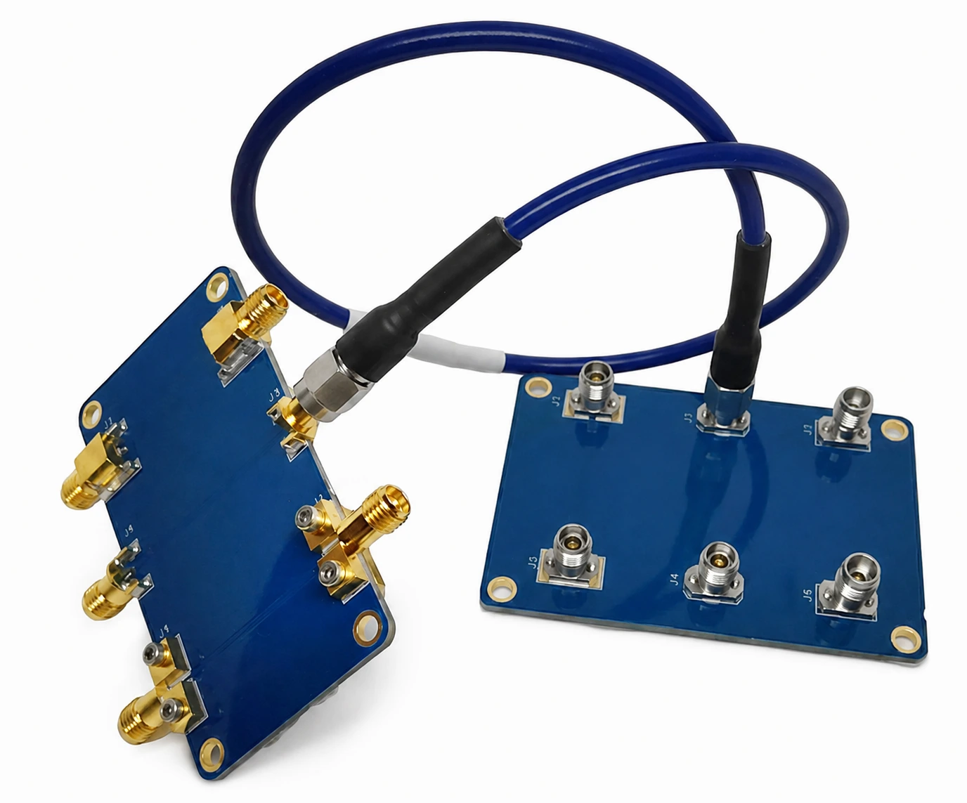
A repeatable solderless fixture should have a defined mechanical procedure rather than relying entirely on technician feel.
The procedure should address connector alignment, mounting hardware, PCB support, connector and landing-area condition, cable attachment, and the measurement reference plane.
It should also define what constitutes an unacceptable condition. That might include visible PCB damage, abnormal connector seating, damaged mounting hardware, or measurement variation outside the fixture’s established acceptance limits.
There is no need to invent a universal specification for those limits.
A 20 GHz fixture and a 67 GHz fixture may not have the same sensitivity. A development fixture used occasionally may also have different maintenance requirements from a production test system that is serviced frequently.
The installation process should follow the measurement need.
Engineering Checklist for Repeatable Solderless Installation
Before relying on repeated connector removal and installation in a high-frequency test fixture, review the following:
- Connector alignment: Can the signal contact and PCB launch be positioned consistently?
- Mounting condition: Is the installation procedure appropriate to the actual connector design?
- Contact condition: Are the connector contact surfaces and mechanical features acceptable for reuse?
- PCB landing area: Are the signal and ground contact regions clean and free from abnormal damage?
- PCB support and flatness: Is uncontrolled board deflection avoided around the connector?
- Fastening process: Is the same mounting sequence and appropriate tooling used each time?
- Cable attachment: Can mating torque or cable stress disturb connector position?
- Measurement reference: Are calibration and de-embedding conditions controlled between comparisons?
- Acceptance criteria: Has acceptable measurement variation been defined for the actual application?
Repeatability Is a Property of the Installed System
Solderless mounting can make a high-frequency test fixture easier to service and modify. A connector may be replaced without desoldering, and a PCB can be reworked without permanently committing the RF interface during early fixture development.
Those advantages are real, but they should not be confused with guaranteed measurement repeatability.
Repeatability depends on recreating the installed RF structure closely enough to meet the application’s measurement criteria.
That includes the connector, PCB launch, alignment, mounting condition, board support, contact surfaces, cable loading, and measurement procedure.
Removability is a mechanical feature. Repeatability is a system-level measurement outcome.
For high-frequency fixtures, both should be considered during the design stage—not after inconsistent measurements begin to appear.
For available Vinstronics 1.0 mm, 1.85 mm, 2.4 mm, and 2.92 mm solderless vertical launch configurations, see the
Solderless Vertical Launch PCB Connectors
platform.
Discuss Your Fixture Repeatability Requirements
If your fixture requires repeated connector removal, PCB rework, connector replacement, or frequent DUT access, the installation procedure should be reviewed together with the RF launch.
Useful information includes the connector interface, target measurement bandwidth, PCB thickness and stack-up, mounting constraints, expected reinstallation workflow, and required measurement repeatability.