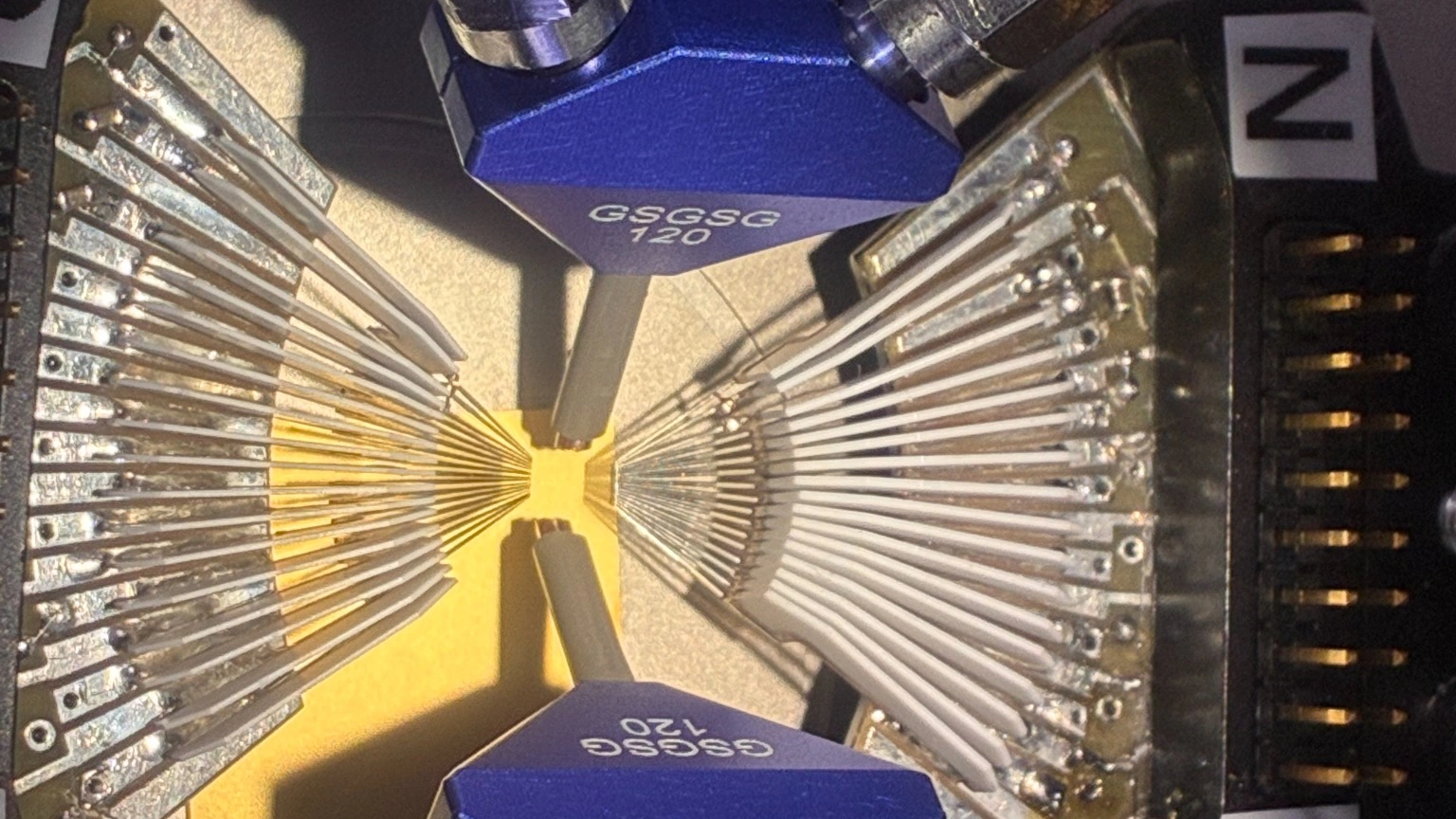
For high-speed PCB testing, both 1.85 mm and 2.92 mm solderless vertical launch connectors can provide direct coax-to-board access without routing the measurement path to the PCB edge.
The real engineering question, however, is not simply which connector has the higher frequency rating.
The key question is: Does the test fixture actually need to move from a 40 GHz measurement interface to a 67 GHz measurement interface?
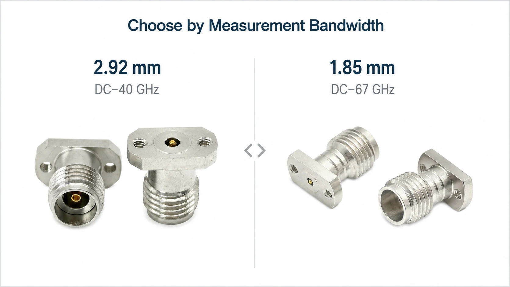
Within the Vinstronics vertical launch range, 2.92 mm interfaces cover applications to 40 GHz, while 1.85 mm interfaces extend to 67 GHz. The additional bandwidth of 1.85 mm can be valuable in higher-bandwidth SerDes, optical-module, signal-integrity and wideband RF characterization, but it does not mean every high-speed digital test automatically requires a 1.85 mm interface.
The better approach is to define the required measurement bandwidth, review the complete test chain, and then select the connector interface that provides appropriate performance and margin.
Short answer: Choose 2.92 mm when the required measurement bandwidth remains comfortably within 40 GHz and it matches the existing test environment. Move to 1.85 mm when the application requires measurements beyond 40 GHz, additional bandwidth headroom, or compatibility with higher-frequency instrumentation and fixtures.
For the complete product family, see the Vinstronics
Solderless Vertical Launch PCB Connectors.
1.85 mm vs. 2.92 mm Vertical Launch Connectors at a Glance
| Selection Factor | 2.92 mm Vertical Launch | 1.85 mm Vertical Launch |
|---|---|---|
| Frequency Coverage | DC–40 GHz | DC–67 GHz |
| Typical Test Focus | RF and general high-speed PCB characterization | Higher-bandwidth digital, optical-module and precision RF characterization |
| Bandwidth Headroom | Suitable when the measurement plan remains within the 40 GHz range | Additional headroom for measurements extending beyond 40 GHz |
| PCB Integration | Vertical solderless compression mount | Vertical solderless compression mount |
| Typical Selection Logic | Use when 40 GHz is sufficient for the complete test path | Use when additional measurement bandwidth is required |
The table is a starting point rather than a substitute for model-level review. Final performance depends on the specific connector, PCB launch, board stack-up, mounting condition and complete measurement environment.
The Main Difference Is Measurement Bandwidth — Not Data Rate Alone
One of the most common mistakes in high-speed digital testing is to select an RF interface by looking only at the nominal serial data rate.
A label such as 112G or 224G describes the digital signaling system. It does not, by itself, define the exact RF bandwidth that every fixture, connector, cable and measurement instrument must support.
The required measurement span depends on what the engineer is trying to characterize. Examples include:
- channel insertion loss and return loss,
- fixture and PCB transition characterization,
- transmitter and receiver validation,
- signal-integrity margin analysis,
- de-embedding requirements,
- instrument bandwidth, and
- the amount of frequency-domain margin required by the test methodology.
This is why a 2.92 mm connector should not automatically be rejected simply because the platform is described as “high speed,” and a 1.85 mm connector should not automatically be specified solely because a design uses a newer SerDes generation.
The correct sequence is:
Define the measurement bandwidth → review the complete test chain → select the RF interface → verify the PCB launch.
When Is a 2.92 mm Vertical Launch Interface Enough?
A 2.92 mm vertical launch connector is often the more practical choice when the required measurement range remains within 40 GHz and the surrounding test equipment is already based on the same interface ecosystem.
Typical situations include:
- RF and microwave PCB characterization within the 40 GHz range,
- high-speed digital fixtures where the required measurement bandwidth does not extend beyond 40 GHz,
- evaluation boards and reusable laboratory fixtures,
- test setups standardized around 2.92 mm instrumentation and cable interfaces, and
- applications where additional 67 GHz capability would not provide a meaningful measurement benefit.
In these cases, moving to a higher-frequency connector simply because it has a higher numerical bandwidth may add cost and interface complexity without improving the actual measurement.
If the complete measurement plan fits comfortably within the 2.92 mm bandwidth range, 2.92 mm remains a technically valid high-frequency test interface.
See the Vinstronics
2.92 mm Vertical Launch Connector
range for available configurations.
When Does Moving to 1.85 mm Make More Sense?
The case for 1.85 mm becomes stronger when the measurement requirement extends beyond the practical bandwidth of a 2.92 mm interface.
With frequency coverage to 67 GHz in the Vinstronics vertical launch range, 1.85 mm provides additional measurement headroom for applications such as:
- higher-bandwidth SerDes characterization,
- optical-module electrical test platforms,
- signal-integrity channel characterization,
- high-frequency semiconductor evaluation boards,
- wideband VNA measurements, and
- fixtures where future measurement requirements may extend beyond 40 GHz.
The practical value of the 1.85 mm interface is therefore not simply that “67 GHz is higher than 40 GHz.” Its value is the ability to preserve additional measurement bandwidth through the connectorized portion of the fixture.
This can become particularly important when the connector and PCB launch are part of a fixture that must be characterized, de-embedded or reused across multiple measurement conditions.
See the Vinstronics
1.85 mm Vertical Launch Connector
range for available configurations.
Moving from 40 GHz to 67 GHz Affects More Than the PCB Connector
Changing from a 2.92 mm interface to a 1.85 mm interface is not always a one-component decision.
The connector sits inside a complete RF measurement chain:
Instrument → Test Cable → Adapter / Calibration Interface → Fixture Connector → PCB Launch → DUT
If the required bandwidth moves toward 67 GHz, engineers should confirm that the rest of the measurement path supports the same frequency range with acceptable loss, return loss and repeatability.
This may include reviewing:
- VNA or measurement-instrument frequency range,
- test-port interface,
- RF test cable bandwidth,
- adapters and inter-series transitions,
- calibration standards or calibration method,
- fixture architecture, and
- PCB launch performance.
For this reason, the decision to move from 40 GHz to 67 GHz should be evaluated at the measurement-system level, not only at the connector level.
The Connector Is Only Part of the PCB Launch
Choosing a 67 GHz connector does not automatically create a 67 GHz PCB transition.
At higher frequencies, the measured transition includes the connector contact, PCB signal pad, reference ground, via field, transmission-line structure and local stack-up. Mechanical alignment and mounting condition also become part of the RF interface.
Important PCB inputs include:
- PCB thickness and local stack-up,
- transmission-line structure such as microstrip or grounded coplanar waveguide (GCPW),
- signal-pad geometry,
- ground-via arrangement,
- available mounting area,
- connector contact position, and
- target measurement frequency.
This is why connector selection and PCB launch design should be reviewed together rather than treated as two unrelated tasks.
If the main design decision is whether the RF signal should leave the PCB from the edge or vertically through the board surface, see our separate guide:
End Launch vs. Vertical Launch RF Connectors for PCB Testing.
1.85 mm vs. 2.92 mm for Optical Module Test Platforms
Optical-module test boards are a good example of why connector selection should be based on the measurement architecture rather than a single product label.
High-speed module test platforms may require multiple RF access points around an OSFP, QSFP-DD or similar module interface. Vertical launch connectors allow these measurement ports to be positioned at required PCB locations without forcing every signal path to the board edge.
For a platform whose required measurement bandwidth remains within 40 GHz, a 2.92 mm solution may be sufficient. When the measurement plan extends beyond that range, a 1.85 mm interface provides bandwidth to 67 GHz and additional room for higher-frequency characterization.
The appropriate choice depends on the actual test points, instrument interfaces, fixture losses, de-embedding strategy and the frequency range that must be preserved through the complete measurement path.
What About 112G and 224G SerDes Testing?
For SerDes validation, avoid selecting the connector from the data-rate number alone.
Instead, start by defining:
- the frequency range required by the measurement,
- whether the test is focused on channel characterization, transmitter validation, receiver testing or fixture verification,
- the bandwidth of the VNA, oscilloscope or other instrumentation,
- fixture loss and de-embedding strategy, and
- the required measurement margin above the primary frequency range of interest.
A 2.92 mm vertical launch may be appropriate for measurements contained within 40 GHz. A 1.85 mm interface becomes more appropriate when the required measurement span extends beyond that range or when additional bandwidth margin is part of the test strategy.
Do not use the rule “112G = 2.92 mm” or “224G = 1.85 mm.”
The required RF interface should follow the measurement bandwidth and fixture architecture, not the data-rate label by itself.
Selection Checklist: 1.85 mm or 2.92 mm?
Before choosing the connector interface, review these questions:
- What is the highest frequency that must actually be measured?
- How much bandwidth margin is required above that range?
- What RF interface is used by the measurement equipment?
- What interfaces are used by the test cables and calibration hardware?
- What PCB stack-up and transmission-line structure will be used at the launch?
- Is the PCB launch itself capable of supporting the required bandwidth?
- Will the fixture need to support future higher-bandwidth DUTs?
If the required measurement bandwidth remains comfortably within 40 GHz, start by evaluating a 2.92 mm solution. If the measurement requirement extends beyond 40 GHz or additional bandwidth headroom is important, evaluate a 1.85 mm solution.
Frequently Asked Questions
Is 1.85 mm always better than 2.92 mm for high-speed PCB testing?
No. A higher-frequency interface is not automatically the better engineering choice. If the required measurement bandwidth is within 40 GHz and the complete test setup is already based on 2.92 mm interfaces, a 2.92 mm vertical launch connector may be the more appropriate solution.
Can a 2.92 mm vertical launch connector be used for SerDes testing?
Yes, when the required measurement bandwidth fits within the connector and fixture bandwidth. SerDes data rate alone does not determine the connector interface.
When should I move from 2.92 mm to 1.85 mm?
Consider 1.85 mm when measurements need to extend beyond the 40 GHz range, when additional bandwidth margin is required, or when the surrounding instrumentation and fixture architecture are designed for higher-frequency characterization.
Does a 67 GHz connector guarantee a 67 GHz PCB launch?
No. The connector is only one part of the transition. PCB stack-up, signal pad, grounding, via geometry, transmission-line structure, mounting condition and connector model all affect the final launch performance.
Need Help Choosing the Interface?
If you are deciding between 1.85 mm and 2.92 mm for a vertical launch test fixture, send the target measurement bandwidth, PCB thickness, stack-up, transmission-line structure and available mounting area.
Vinstronics can review the application and help identify a suitable vertical launch interface and connector configuration.
Related:
Solderless Vertical Launch PCB Connectors
·
End Launch vs. Vertical Launch RF Connectors