Engineering Problem:
A request such as “We need a 67 GHz SS probe” identifies the electrical platform, but it does not define whether the probe can land accurately and repeatedly on the PCB. Signal pitch, pad dimensions, exposed metal area, approach direction, and nearby mechanical clearance are part of the probe specification.
Selecting an SS differential RF probe requires more than choosing the highest frequency rating. The probe configuration must match the actual PCB landing geometry.
Frequency selects the electrical platform. PCB pad geometry defines the physical probe configuration. Provide the signal-pad center-to-center pitch, individual pad dimensions, solder-mask opening, target frequency, approach direction, and a dimensional drawing before the final configuration is confirmed.
Vinstronics provides DC–40 GHz and DC–67 GHz SS differential probe platforms with 100 Ω differential impedance and application-specific pitch configurations within the supported 350–3000 µm range.
For guidance on selecting between SS and GSSG landing formats, see SS vs. GSSG RF Probes for Differential PCB Testing. For situations without practical local ground pads, see SS RF Probes for PCB Testing Without Local Ground Pads.
30-Second Specification Check
| Information Required | Correct Definition | Common Mistake |
|---|---|---|
| Signal pitch | Center of S+ pad to center of S− pad | Measuring the empty gap between pads |
| Pad size | Width and length of each copper pad | Providing only the pitch |
| Exposed landing area | Metal area available after solder-mask coverage | Assuming the full copper pad is contactable |
| Approach direction | Direction from which the probe reaches the pads | Ignoring nearby components or fixture walls |
| Frequency range | Required measurement bandwidth | Selecting the highest-frequency probe by default |
Tip Size, Pad Size, Pitch and Landing Area
These four dimensions describe different parts of the probing interface and should not be used interchangeably.
Tip Size
The physical dimension of each individual contact tip. The published Vinstronics SS probe tip-size value is 120 µm.
Pad Size
The width and length of each copper test pad before solder-mask and tolerance effects are considered.
Pitch
The center-to-center distance between the two signal pads and the two signal contacts.
Effective Landing Area
The exposed metal region remaining after solder-mask coverage, fabrication tolerance, alignment variation, and nearby-feature clearance are considered.
120 µm Tip Size Is Not 120 µm Pitch
The SS contact-tip dimension and the signal-to-signal spacing are separate parameters. A 120 µm tip does not imply a 120 µm signal pitch.
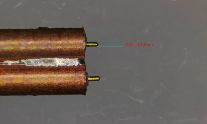
For example, VST-D67G-SS-800 identifies a DC–67 GHz SS probe configured for an 800 µm signal-to-signal pitch. The suffix “800” describes the pad pitch, not the tip size.
How to Measure SS Probe Pitch Correctly
For an SS probe, measure from the center of the positive signal pad to the center of the negative signal pad.
Provide These Dimensions
- Center-to-center signal pitch
- Individual pad width and length
- Solder-mask opening
- Differential-pair orientation
- Nearby vias and copper
- Intended probe approach direction
Do not provide only the edge-to-edge gap. For irregular, offset, or asymmetric pads, provide the original CAD or Gerber data rather than estimating the pitch from a photograph.
Why Correct Pitch Alone Is Not Enough
Matching the probe pitch to the PCB pitch is necessary, but it does not prove that the complete landing geometry is suitable.
An 800 µm configuration may still require engineering review when:
- One pad is narrower or shorter than the other
- The two pads are longitudinally offset
- Part of a pad is covered by solder mask
- A via enters the expected contact region
- Nearby components restrict the probe body
- The test point cannot be approached along a suitable axis
- The two landing points are not on the same local plane
Engineering Check
The correct question is not only “Does the pitch match?” It is “Can both tips land within the exposed metal area with adequate positioning tolerance and mechanical clearance?”
Pad Size, Solder Mask and Nearby Features
The nominal copper-pad outline does not always represent the usable contact area. Solder mask, fabrication tolerances, rounded corners, vias, and adjacent copper can reduce the available landing region.
Landing too close to the exposed-pad edge may increase the risk of:
- Sliding outside the metal area
- Contacting solder mask
- Reaching adjacent copper
- Producing inconsistent contact resistance
- Creating different landing marks after repeated touchdowns
There is no single universal pad margin that applies to every probe and fixture. The required margin depends on the contact structure, positioning system, PCB geometry, and test conditions.
Mechanical access must also be reviewed. Potential obstructions include tall components, shielding cans, connector housings, heat sinks, fixture walls, adjacent probes, microscope restrictions, and RF cable-bend limits.
The 45-degree connector arrangement used on the Vinstronics SS platform helps with cable clearance, but it does not remove the need to evaluate the complete setup.
Configurable Pitch Does Not Mean Field-Adjustable Pitch
The Vinstronics SS platform supports pitch configurations within a range of 350–3000 µm.
This means that probes can be supplied for different PCB pad layouts within the supported platform. It does not mean that one fixed probe can be continuously adjusted between 350 and 3000 µm during use.
Each probe is configured for:
- A defined signal-pad pitch
- A defined contact geometry
- A corresponding model suffix
- The intended measurement and verification setup
Different configurations may require configuration-specific characterization, verification, or de-embedding data depending on the required measurement accuracy and reference plane.
What “XXX” Means in the Model Number
VST-D40G-SS-XXX
VST-D67G-SS-XXX
- D40G = DC–40 GHz platform
- D67G = DC–67 GHz platform
- SS = Signal-Signal contact configuration
- XXX = Required signal-pad pitch in microns
Example:
DC–67 GHz SS differential probe configured for an 800 µm signal-pad pitch.

Selecting the 40 GHz or 67 GHz Platform
The electrical platform should be selected after the landing geometry has been reviewed.
| Model Series | Frequency | RF Interface | Differential Impedance | Pitch Range |
|---|---|---|---|---|
| VST-D40G-SS-XXX | DC–40 GHz | 2.92 mm Female | 100 Ω | 350–3000 µm |
| VST-D67G-SS-XXX | DC–67 GHz | 1.85 mm Female | 100 Ω | 350–3000 µm |
Do not select the 67 GHz version only because it has the higher frequency rating. The usable measurement bandwidth depends on the complete path:
The appropriate platform is the one that supports the required analysis bandwidth without adding unnecessary interface or setup complexity. For the cable side of the measurement path, see Vinstronics RF cable assemblies.
Practical Specification Examples
Example 1: Defined 800 µm S-S Pads
Two equal signal pads, 800 µm center-to-center pitch, clear solder-mask openings, adequate approach space, and no practical local ground pads. A VST-D40G-SS-800 or VST-D67G-SS-800 may be considered, depending on the required bandwidth.
Example 2: Pitch Matches, Landing Geometry Does Not
The signal pitch is correct, but one pad is short, asymmetric, partly masked, close to a via, or obstructed by nearby components. Pitch alone is not sufficient. Submit the dimensional pad drawing, board photograph, and approach direction for review.
Example 3: Several PCB Versions Use Different Pitches
Boards use 500, 800, and 1500 µm signal spacing. The supported platform range does not mean one probe can move between all three layouts. Review separate configured probes or an application-specific contact solution.
Common Specification Mistakes
- Providing only the target frequency: “We need a 67 GHz probe” does not define the mechanical contact structure.
- Measuring edge-to-edge spacing: Pitch should be specified center to center.
- Treating tip size as pitch: A 120 µm tip does not mean 120 µm signal spacing.
- Ignoring solder-mask opening: The exposed landing area may be smaller than the copper pad.
- Assuming one probe covers the full pitch range: Each probe is supplied for a defined layout.
- Ignoring approach direction: Correct pad spacing is insufficient if nearby hardware blocks the probe or cable path.
What to Send for Engineering Review
- PCB pad drawing or Gerber excerpt
- Clear top-view photograph
- Signal-to-signal center pitch
- Individual pad width and length
- Solder-mask opening dimensions
- Differential impedance and target frequency
- DUT type and probe approach direction
- Nearby component and fixture clearance
- Probe station or automated tester information
- VNA, RF interface, and calibration or de-embedding requirements
A target frequency and general photograph may be sufficient for an initial discussion, but dimensional PCB information is required before the final configuration is confirmed.
Conclusion
An SS RF probe should not be selected from frequency alone.
The correct process is:
- Confirm that the landing pattern is S-S.
- Measure the signal pitch center to center.
- Verify the width and length of each pad.
- Check the exposed landing area.
- Review solder mask and nearby features.
- Confirm probe and cable access.
- Select the required 40 GHz or 67 GHz platform.
- Define the model using the required signal pitch.
Match the probe to the real PCB landing geometry—not only to the bandwidth requirement.
FAQ
What is the difference between SS probe tip size and pitch?
Tip size describes the individual contact end. Pitch is the center-to-center spacing between the two signal tips.
How should SS probe pitch be measured?
Measure from the center of one signal pad to the center of the other signal pad.
Can one SS probe cover every pitch from 350 to 3000 µm?
No. The platform supports configurations within that range, but each probe is configured for a defined pad pitch.
What does 800 mean in VST-D67G-SS-800?
It identifies an 800 µm signal-to-signal pad pitch.
Is a PCB photograph enough for probe selection?
A photograph is useful for initial review, but a dimensional pad drawing or Gerber excerpt is preferred before the final configuration is confirmed.
Does the correct pitch guarantee reliable contact?
No. Pad dimensions, solder-mask opening, landing tolerance, mechanical clearance, and approach direction must also be reviewed.
Should I select the 67 GHz probe instead of the 40 GHz version?
Select the platform according to the required bandwidth, VNA capability, RF interfaces, and complete measurement-chain performance—not simply the highest available frequency.
Need an SS Probe Configuration Review?
Send the center-to-center pitch, pad dimensions, solder-mask opening, target frequency, and a clear image or drawing of the test area. Vinstronics engineers can review the suitable SS probe configuration before quotation.