An SS probe becomes useful only when its contact geometry can be translated into a controlled PCB measurement.
In practice, this means more than matching two signal contacts to two differential landing positions. Probe alignment, mechanical access, PCB geometry and the complete RF measurement path all become part of the measurement.
The images below show a practical SS probing setup, the Signal-Signal contact structure, an actual PCB landing and a VNA measurement with the displayed sweep extending to 40 GHz.
This is not presented as a complete characterization report for a specific probe configuration. The purpose is to show how SS probing is implemented in a real board-level measurement environment and which engineering factors matter at the probe-to-PCB interface.
Practical SS RF Probing on a Differential PCB
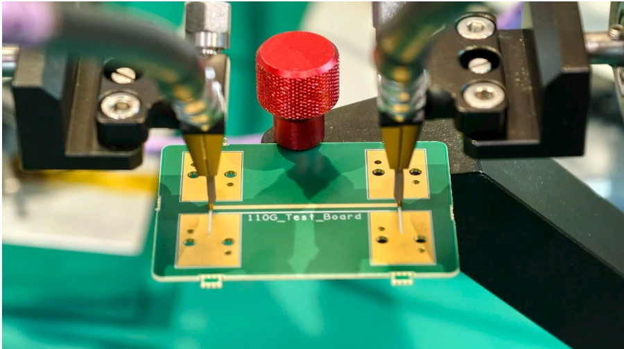
The setup shows RF probes positioned over a PCB test structure using mechanical probe positioners.
In an actual measurement, the probe must reach the intended landing area without interference from the positioner, nearby structures or the RF cable path. Cable loading should also be controlled so that it does not disturb the probe position after contact is established.
This mechanical arrangement is part of the measurement setup, not merely a fixture for holding the probe.
Understanding the SS Contact Geometry
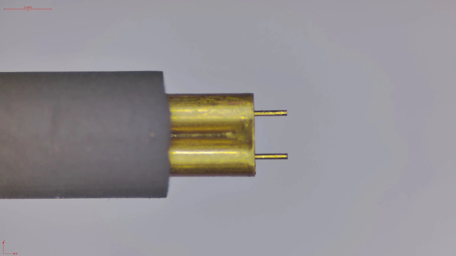
An SS probe presents two signal contacts to the DUT landing structure. The spacing of those contacts must correspond to the intended differential landing geometry on the PCB.
Two dimensions should not be confused:
- Contact or tip geometry describes the physical geometry of the individual probe contacts.
- Pitch describes the center-to-center relationship between the two signal contacts and must be selected for the DUT layout.
A probe platform may support multiple pitch configurations, but an individual probe is manufactured for the specified DUT geometry. A published pitch range therefore does not mean that one probe is continuously adjustable across that range.
For the mechanical selection process, see How to Specify an SS RF Probe from PCB Pad Geometry.
Landing the Probe on the Differential PCB Structure
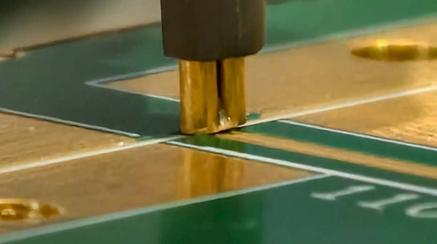
The probe-to-PCB landing is the point where the mechanical contact geometry becomes part of the RF transition.
Correct pitch alone is not sufficient. The engineer also needs to consider the exposed conductive area, solder-mask opening, local trace geometry and physical clearance around the landing site.
The close-up image shows the two probe contacts positioned on the PCB transmission structure. For repeatable measurement, both contacts need to land within the intended conductive regions under a consistent contact condition.
A shift in landing position changes the local probe-to-PCB interface. At microwave frequencies, that interface should therefore be treated as part of the measured transition rather than as an ideal electrical connection.
Why SS Probing Can Simplify Differential Landing
An SS landing removes the requirement for dedicated local ground contacts at the probe landing site. It does not remove the electromagnetic return path from the measurement.
The return-current distribution is still determined by the DUT structure and its surrounding reference environment.
This is why SS and GSSG should not be treated as interchangeable probe topologies. The appropriate choice depends on the DUT landing structure, return-path implementation and measurement objective.
For the topology-selection question, see SS vs. GSSG RF Probes for Differential PCB Testing: How to Choose.
Example VNA Measurement Extending to 40 GHz
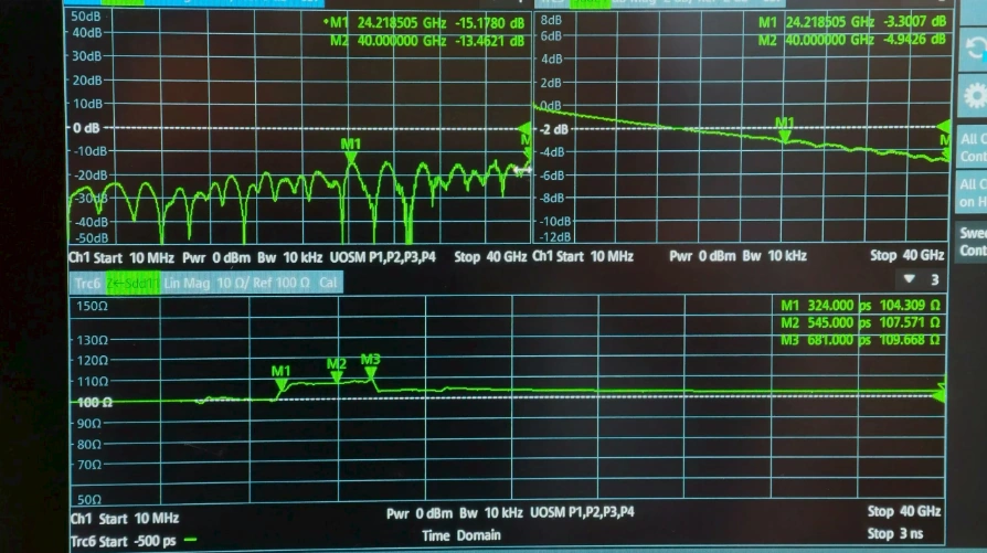
The VNA display shown here contains multiple measurement traces and markers, with the displayed frequency sweep extending to 40 GHz.
The image demonstrates the SS probe being used within an RF measurement setup. It is not presented here as a complete published performance characterization for a specific probe configuration.
Interpreting the displayed response requires knowledge of the complete measurement conditions, including calibration, reference plane, interconnect path, PCB transition and DUT. For that reason, no individual trace in this image is being assigned a performance specification in this article.
The usable measurement bandwidth is determined by the complete path rather than by the probe rating alone.
For a detailed discussion of bandwidth-platform selection, see 40 GHz vs. 67 GHz SS Differential RF Probes: How to Choose for PCB Testing.
What Engineers Should Verify Before Measurement
A practical SS measurement review should cover six areas before the probe is landed on the DUT:
- DUT landing geometry: confirm that the exposed conductive regions and differential spacing match the intended probe configuration.
- Probe pitch and contact configuration: verify that the physical contact arrangement corresponds to the PCB layout.
- Mechanical clearance: check probe-body, positioner and cable access around the landing site.
- Landing repeatability: establish a consistent contact condition for repeated measurements.
- Complete RF interconnect path: confirm that the instrument, cables, interfaces and PCB transition support the intended measurement range.
- Calibration and reference plane: define the correction plane according to the measurement objective.
De-embedding, when used, should be treated as a separate operation for removing a characterized network. It does not replace VNA calibration.
What This Example Shows — and What It Does Not
| This Example Shows | It Does Not Establish |
|---|---|
| Real SS probe setup on a PCB test structure | Universal performance for every SS probe configuration |
| Physical Signal-Signal contact geometry | A single pitch or contact geometry for all DUT layouts |
| Actual probe-to-PCB landing | Complete mechanical tolerances or setup limits |
| A VNA display with the sweep extending to 40 GHz | Published 40 GHz S-parameter limits for every configuration |
| A practical RF measurement environment | The calibration or de-embedding procedure used for a specific measurement |
From Probe Selection to Practical Measurement
Each stage affects the next.
Selecting SS instead of GSSG addresses the contact topology. Defining the probe pitch addresses the physical relationship between the probe and the DUT. Selecting a 40 GHz or 67 GHz platform addresses the required electrical bandwidth and RF interface environment.
The practical measurement brings these decisions together at the probe-to-PCB transition.
This is why probe selection should begin with the DUT and the intended measurement rather than with the highest available frequency specification.
Conclusion
An SS differential RF probe provides a direct two-signal contact interface for compatible PCB and PCBA differential structures.
In practical use, the probe-to-PCB landing, mechanical positioning and complete RF interconnect path are all part of the measurement. The images shown here illustrate that progression from the physical SS contact structure to actual PCB landing and a VNA measurement with the displayed sweep extending to 40 GHz.
For engineers evaluating an SS probing approach, the useful starting point is to review the DUT landing geometry, required measurement bandwidth and complete RF test path together.
FAQ
Does an SS RF probe require local ground needles?
No dedicated local ground needles are used at the SS landing area. However, this does not mean that the measurement has no electromagnetic return path. The DUT structure and its surrounding reference environment remain part of the differential measurement system.
Is probe pitch the same as tip size?
No. Tip or contact geometry describes the physical contact itself, while pitch describes the spacing relationship between the two signal contacts.
Does a VNA sweep to 40 GHz prove that every SS probe configuration is fully characterized to 40 GHz?
No. A displayed measurement sweep is not a substitute for a complete characterization report. Probe configuration, calibration, RF path, PCB transition and measurement conditions must all be considered.
Can an SS probe replace a GSSG probe in every differential measurement?
No. SS and GSSG are different contact topologies. The appropriate choice depends on the DUT landing structure, available local ground landing positions, return-path implementation and measurement objective.
What should be reviewed before ordering an SS RF probe?
The DUT signal-pad geometry, required pitch, available landing area, mechanical access, required measurement bandwidth and RF interface environment should be reviewed together.
Need an SS Probe Configuration Review?
Send your PCB landing layout, required measurement bandwidth and RF interface requirements. Vinstronics can review the suitable SS probe configuration for your application.