In the semiconductor manufacturing landscape, wafer testing is a pivotal step that ensures quality control and performance assessment of chips before packaging. This article delves into the definition, purpose, significance, and types of wafer testing, as well as the critical role and importance of RF Probes in this process.
What is Wafer Testing
Wafer testing, also known as wafer probing or chip probing (CP), is the process of electrically testing each bare die on a wafer before it is packaged. It involves assessing the basic functionality and performance of the chips against design specifications.

Purpose of Wafer Testing
- Quality Control: Identifying qualified chips to improve yield rates.
- Performance Assessment: Evaluating the electrical characteristics of devices/circuits.
- Feedback for Improvement: Providing comprehensive performance feedback for process enhancement.
Importance of Wafer Testing
Cost Savings: Eliminating defective chips before packaging.
Quality Data: Offering valuable data on manufacturing process quality.
Process Improvement: Facilitating process improvement and product reliability assessment.

Types of Wafer Testing
Wafer Acceptance Test (WAT)
This test is conducted to ensure the quality and stability of the semiconductor manufacturing process before the wafers proceed to further processing.
Chip Probing (CP)
Also known as Wafer Probing, this test filters out electrically non-functional chips before packaging, saving costs associated with further processing of defective chips.
Electrical Parameter Monitoring (EPM)
This involves measuring the electrical characteristics of individual elements on the wafer to provide feedback on the manufacturing process.
Wafer Burn-in
Designed to identify early failures in the chips, reducing the likelihood of customer dissatisfaction and product returns due to defects.
DC Test, AC Test, and Function Test
These tests verify direct current and voltage parameters, operational characteristics such as input and output transition times, and logical functions of the chips, respectively.
Optical and Electron Beam Inspection
Used for defect detection on the wafer surface, with optical inspection being the primary method due to its speed and efficiency, while electron beam inspection is used for its high resolution in R&D and process development.
Particle and Surface Defect Detection
This involves detecting and counting particles and contaminants on the wafer surface, as well as identifying defects and contamination through optical and laser scanning methods.
Equipment for Wafer Testing
- Automatic Test Equipment (ATE): Also known as a tester, the ATE is crucial for detecting the function and performance of chips, including semiconductor devices’ circuit functions and electrical performance parameters .
- Wafer Prober: The prober is used in conjunction with the ATE to test the functionality and electrical parameters of bare dies on the wafer .
- Handler (Prober): The handler, or prober, is responsible for the transportation and alignment of the wafer during the testing process .
- Defect Review SEM (Scanning Electron Microscope): This equipment is used for high-resolution imaging and analysis of the wafer surface to detect defects that may affect the performance of the chips .
- Optical Inspection Equipment: Used for detecting surface defects on the wafer, optical inspection equipment employs advanced optical systems and AI algorithms to identify common defects on the wafer surface .
- Particle Counter: This device is used to count and analyze particles on the wafer surface, which is crucial for maintaining cleanliness and quality standards in semiconductor manufacturing .
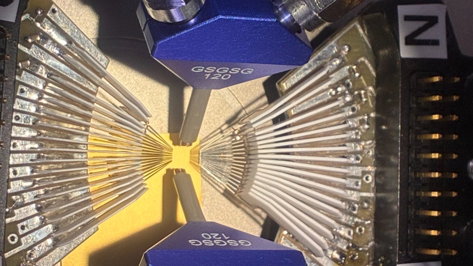
- RF Probe: Specifically designed for testing high-frequency devices on the wafer, the RF probe is integrated into the Wafer Prober setup when testing devices that require RF capabilities .
The Role of RF Probes in Wafer Testing
The role of RF Probes in wafer testing is multifaceted and crucial for the accurate characterization and development of integrated RF technologies.
- Precision Measurement: RF Probes enable precise measurements of electrical parameters such as S-parameters, noise figure, and DC characteristics directly on the wafer, which is vital for assessing a device in its raw, unpackaged state.
- Device Development: They play a key role in almost every stage of RF device development, from technology development and model parameter extraction to design verification and production testing.
- Signal Integrity: RF Probes are designed to minimize electromagnetic interference and maintain signal integrity, especially when dealing with high-frequency applications.
- Contactless Probing: Novel RF probe technologies are being developed to provide contactless RF probing on test structures, showing the path toward continuous measurements across the microwave, millimeter-wave, and Terahertz range.
- Calibration and Accuracy: RF Probes allow for accurate calibration of the measurement reference plane to their tips, canceling out probe losses and reflections from the probe lines and transition to coaxial connector.
- High Contact Repeatability: The high contact repeatability of RF Probes has facilitated the development of probe tips and on-wafer standards, as well as dedicated calibration methods.
- Planarization: RF Probes require tilting to contact the DUT signal and ground pads simultaneously, a procedure known as “probe planarization,” which ensures reliable and repeatable contact.
- MEMS-Based Probes: The impact of tilt-related errors on the positioning of microcantilever-based microelectromechanical systems (MEMS) on-wafer electrical probes is quantified and investigated, showing the importance of RF Probes in high-precision applications.
- Cost and Time Efficiency: By measuring true characteristics of RF components at the wafer level, RF Probes have halved research and development times and lowered the costs of developing new products.
These roles underscore the indispensable nature of RF Probes in the field of semiconductor testing, particularly in the realm of RF and microwave device characterization.
Importance of RF Probes
The importance of RF Probes in semiconductor testing and high-precision applications can be summarized as follows:
- Early Defect Detection: RF on-wafer measurements allow engineers to pinpoint defects early in the production process, reducing costs and streamlining production with automated testing that ensures speed and accuracy.
- Intrinsic Properties Assessment: RF wafer probing is critical for understanding the intrinsic properties of semiconductor devices, which is essential for successful product development and manufacturing.
- Broad Application Range: RF Probes are used in a wide range of applications, including impedance matching, multiport, differential, and mixed-signal measurements up to 110 GHz, temperatures beyond 500°C and down to 4K, high-power measurements up to 60 W in continuous-wave mode, and terahertz (THz) applications up to 750 GHz.
- Research and Development Efficiency: By measuring the true characteristics of RF components at the wafer level, RF probes have halved R&D times and lowered the costs of developing new products.
- Precision and Repeatability: RF Probes, especially those using MEMS technology, offer unmatched accuracy and repeatability, which are crucial for demanding RF and high-power applications.
- Calibration and Measurement Accuracy: Accurate RF measurements rely on rigorous calibration, and RF Probes play a critical role in this process, allowing for the correction of system errors and ensuring reliable results.
- Adaptability to Challenging Surfaces: RF Probes cater to a variety of materials, including challenging surfaces like aluminum, providing versatility in testing different types of devices.
- Enhanced Visibility and Positioning: Advanced RF Probes, such as those with a unique protrusion tip design, offer real-time visibility of the tip contacts, allowing for highly accurate positioning even for inexperienced operators.
- Longevity and Durability: High-quality RF Probes, like Vinstronics RF Probes, are designed to have a long lifespan.

Wafer testing is an indispensable part of semiconductor manufacturing, ensuring quality control and performance assessment before chip packaging. RF Probes play a vital role in testing, especially for wireless communication chips. As technology advances, RF Probe technology continues to evolve to meet the growing testing demands.