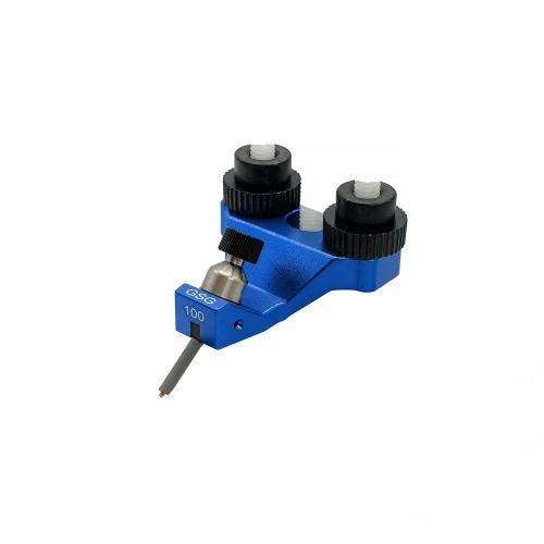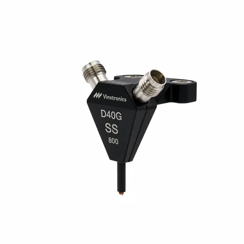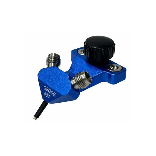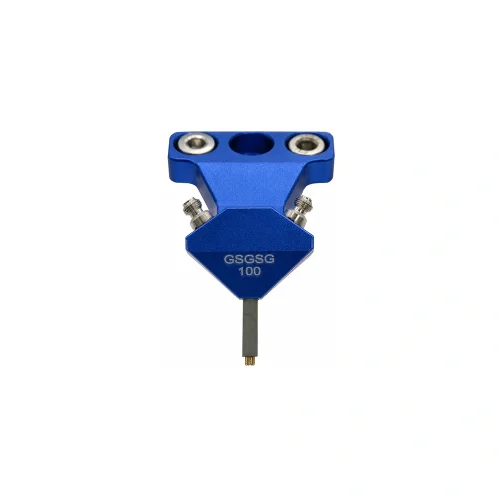
110 GHz GS RF Probe for On-Wafer and PCB Characterization VST-110G-GS

P/N: VST-110G-GS-XXX

  • For single-ended PCB and wafer-level testing
  • GS geometry for clean ground-signal probing
  • Fine-pitch tips for dense pad layouts
  • Well suited to mmWave device validation
  • Supports precision measurements through 110 GHz
Engineering Note
VST-110G-GS is a DC–110 GHz GS RF probe for single-ended on-wafer measurement and high-frequency PCB characterization. It uses a GS tip configuration, 1.00mm female interface, and 45-degree connector angle, with fine-pitch options from 50 μm to 500 μm. This configuration is intended for wafer-level and board-level measurements where low loss, stable contact, and repeatable high-frequency probing are required.

Technical Specifications

Part Number VST-110G-GS-XXX
Product Type GS RF probe
Frequency Range DC–110 GHz
Insertion Loss < 3.0 dB
Return Loss > 12 dB
Impedance 50 Ω
DC Current ≤ 1 A
DC Voltage ≤ 100 V
RF Power ≤ 5 W
Connector 1.00mm Female
Tip Configuration GS / SG
Connector Angle 45-degree
Pitch Range 100 μm–1250 μm or customized
Standard Pitch Step 50 μm
Tip Size 25 μm for 100–250 μm pitch; 50 μm for 300–1250 μm pitch

Target Applications

Wafer-Level mmWave Characterization
Intended for on-wafer measurement of mmWave devices where fine pitch and stable contact performance are required.
High-Speed IC and Interconnect Characterization
Suitable for chiplet, IC, and interconnect evaluation where single-ended high-frequency probing is required.
Fine-Pitch PCB and R&D Validation
Used for advanced R&D environments requiring fine-pitch probing on compact high-frequency structures and validation platforms.
Engineering Support

Need a Quote or Technical Support?

Share the part number, required quantity and application requirements. Our engineering team can assist with product selection, configuration review and quotation support.

Product selection support
Custom configurations available
Specification and compatibility review

Request a Quick Quote