
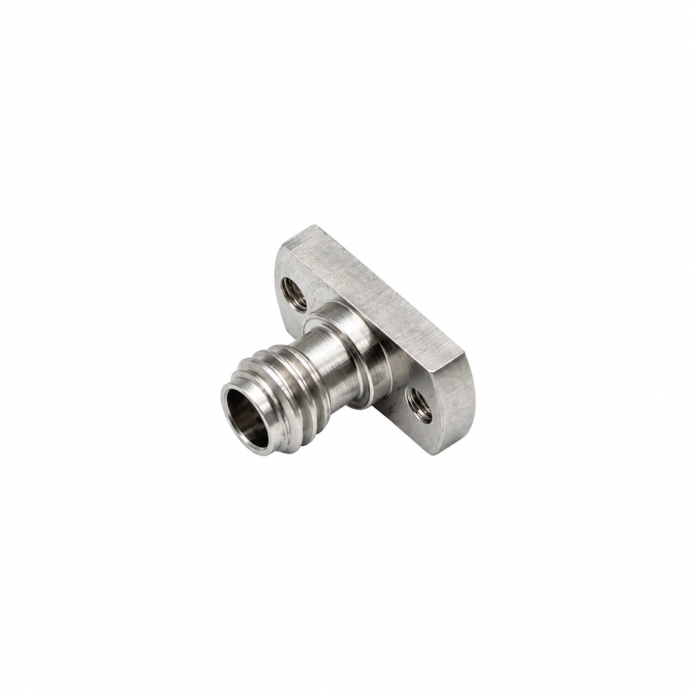
1.0 mm Solderless Vertical Launch PCB Connector, DC–110 GHz | VST-CPM10F-09
P/N: VST-CPM10F-09
• DC–110 GHz Solderless Vertical-Launch PCB Interconnect
• 1.0 mm Female Straight Interface | 50 Ω
• VSWR ≤1.45
• Two-Screw Flange Mounting with Recommended PCB Layout
• Passivated Stainless-Steel Outer Conductor with Gold-Plated BeCu Center Contact
• 7.16 ±0.05 mm Mounting-Hole Spacing | #0-80UNF Hardware
VST-CPM10F-09 is a 50 Ω 1.0 mm female straight PCB connector for solderless vertical-launch integration from DC to 110 GHz. The connector uses a two-screw flange mount, and the mechanical drawing includes a recommended PCB layout for board-level integration.
RF performance is specified at VSWR ≤1.45. The outer conductor and mounting screws are passivated stainless steel, the center conductor is gold-plated beryllium copper, and the dielectric is PEI.
DC–110 GHz Solderless Vertical Launch
Broadband 50 Ω PCB interconnection for RF and millimeter-wave designs through 110 GHz.
1.0 mm Female Straight Interface
Precision 1.0 mm female coaxial interface for vertical board-level connectivity.
VSWR ≤1.45
Maximum specified VSWR of 1.45 across the rated DC–110 GHz frequency range.
Two-Screw Flange Mounting
Two #0-80UNF mounting screws provide the defined mechanical attachment shown in the drawing.
Recommended PCB Layout Provided
The mechanical drawing includes mounting-hole locations and detailed center launch geometry for integration review.
Precision Metal & Contact Construction
Passivated stainless-steel outer conductor with a gold-plated BeCu center conductor and PEI dielectric.
| Part Number | VST-CPM10F-09 |
|---|---|
| Connector Type | 1.0 mm Female, Straight PCB Connector |
| Impedance | 50 Ω |
| Frequency Range | DC–110 GHz |
| VSWR | ≤1.45 |
| Dielectric Withstand Voltage | 500 Vrms |
| Insulation Resistance | 5000 MΩ |
The supplied mechanical drawing includes a Recommended PCB Layout for the two-screw flange mount and center launch region.
Key board references include 2 × Ø1.6 +0.05 mm mounting holes on 7.16 ±0.05 mm centers. The drawing also defines the center launch geometry, including Ø0.3 ±0.05 mm, Ø1.2 ±0.05 mm, and Ø4.25 ±0.05 mm reference diameters. Use the drawing as the dimensional authority for PCB implementation.
| Interface Thread | M4 × 0.7-6g |
|---|---|
| Connector Mounting Threads | 2 × #0-80UNF-2B, through hole |
| Supplied Mounting Screws | 2 × #0-80UNF-2A, separate packing |
| PCB Mounting-Hole Spacing | 7.16 ±0.05 mm |
| PCB Mounting Holes | 2 × Ø1.6 +0.05 mm |
| Overall Axial Length | 6.15 mm |
| Flange Thickness | 1.65 mm |
| Flange Width | 5.8 mm |
| Outer Conductor | Stainless steel, passivated |
| Center Conductor | Beryllium copper, gold-plated |
| Dielectric | PEI |
| Screw | Stainless steel, passivated |
110 GHz PCB Test Fixtures
Precision coaxial access for high-frequency fixtures and PCB-based measurement structures.
Millimeter-Wave Evaluation Boards
Board-level RF connectivity for devices, modules, and test vehicles operating through 110 GHz.
VNA & Component Characterization
High-frequency interface between compatible 1.0 mm test cables and PCB measurement structures.
RF & mmWave R&D
Solderless vertical PCB interconnection for laboratory development and characterization setups.
The recommended PCB layout is included in the mechanical drawing. For a 110 GHz implementation, use the drawing dimensions as the mechanical reference and review the complete PCB stack-up and transition geometry as part of the board-level RF design. The drawing does not define the PCB substrate material or stack-up.
Integrate a 1.0 mm Solderless Vertical Launch into Your 110 GHz Design
Share your PCB stack-up, board thickness, launch geometry, and test requirements for connector selection or technical review.


Need a Quote or Technical Support?
Share the part number, required quantity and application requirements. Our engineering team can assist with product selection, configuration review and quotation support.