
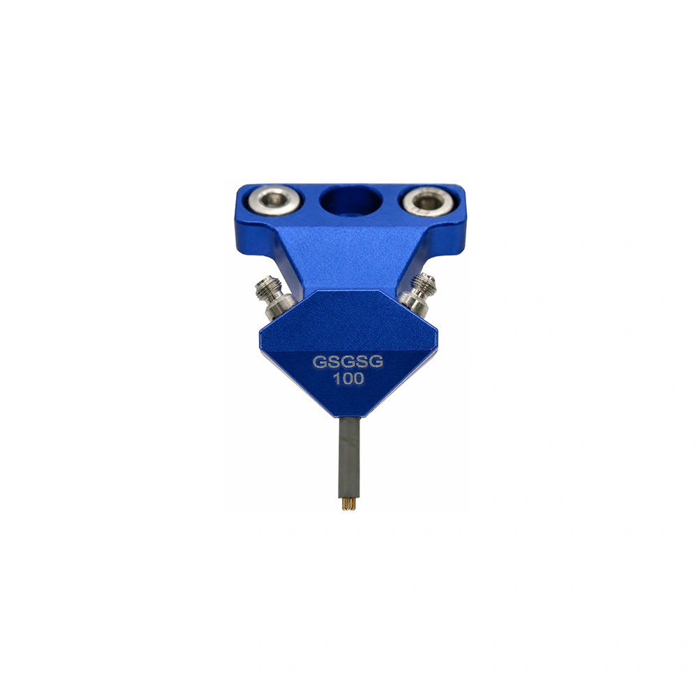
145 GHz GSGSG Differential RF Probe, 100 Ω, 0.8 mm Female | VST-145G-GSGSG-XXX
P/N: VST-145G-GSGSG-XXX
• DC–145 GHz GSGSG probing for differential and mixed-mode characterization
• 100 ±2 Ω differential impedance with <3.5 dB insertion loss and >10 dB return loss
• Interleaved G-S-G-S-G contact geometry for differential RF pad structures
• Configurable 100–1250 μm pitch with 0.8 mm female RF interfaces
• S4P characterization data available to support four-port de-embedding and mixed-mode analysis
VST-145G-GSG-XXX is a 50 Ω Ground-Signal-Ground RF probe for single-ended on-wafer and device characterization from DC to 145 GHz. The probe combines a precision 0.8 mm female RF interface with configurable GSG pitch from 100 μm to 1250 μm for RFIC, MMIC, wafer, package, interconnect, and high-frequency test-structure measurements.
Electrical performance is specified at insertion loss <3.5 dB and return loss >10 dB through 145 GHz, with 50 ±1 Ω impedance control. Pitch selection is configurable to match the DUT pad layout.
DC–145 GHz GSG Probing
Single-ended Ground-Signal-Ground probing for microwave, millimeter-wave, and D-band device characterization.
50 ±1 Ω Impedance Control
Controlled 50 Ω probe impedance supports a consistent transition from the coaxial interface to the GSG contact structure.
<3.5 dB Insertion Loss
Specified insertion loss below 3.5 dB across the DC–145 GHz operating range, with return loss greater than 10 dB.
Configurable 100–1250 μm Pitch
Pitch options cover a broad range of RF pad geometries, with 25 μm steps from 100–250 μm and 50 μm steps from 300–1250 μm.
0.8 mm Female RF Interface
A 45° 0.8 mm female coaxial interface supports integration into 145 GHz probe-station measurement setups.
S-Parameter Support for De-Embedding
Probe characterization data can be supplied in S2P format to support de-embedding and measurement-system integration.
145 GHz falls within the D-band frequency region used for advanced sub-THz component and system research. At these frequencies, probe transition geometry, impedance continuity, pad layout, calibration, and probe-tip contact become increasingly important to the measurement path. The VST-145G-GSG-XXX is designed as a single-ended 50 Ω GSG interface for direct contact to compatible on-wafer and planar RF test structures.
| Part Number | VST-145G-GSG-XXX |
|---|---|
| Frequency Range | DC–145 GHz |
| Tip Configuration | GSG (Ground-Signal-Ground) |
| Impedance | 50 ±1 Ω |
| Insertion Loss | <3.5 dB |
| Return Loss | >10 dB |
| DC Current | ≤1 A |
| DC Voltage | ≤100 V |
| RF Power | ≤5 W |
| RF Connector | 0.8 mm Female |
|---|---|
| Connector Angle | 45° |
| Pitch Range | 100–1250 μm |
| Pitch Step, 100–250 μm | 25 μm |
| Pitch Step, 300–1250 μm | 50 μm |
| Mechanical Envelope | Approx. 37.4 mm body length × 30.0 mm body width, per datasheet outline |
For best measurement accuracy, calibrate the measurement reference plane at the probe tip using a calibration substrate and method compatible with the selected pitch and measurement setup. The datasheet lists SOLT / LRM-compatible calibration substrates as recommended accessories.
S-parameter characterization data can be supplied to support probe de-embedding. De-embedding should be applied according to the VNA, calibration method, reference-plane definition, and DUT measurement workflow used in the test system.
On-Wafer S-Parameter Measurements
Single-ended RF characterization of wafer-level devices and planar GSG test structures through 145 GHz.
RFIC & MMIC Characterization
High-frequency measurement of amplifiers, mixers, passive structures, and other RF/mmWave integrated devices.
D-Band & Sub-THz R&D
Component characterization for D-band research, including emerging high-frequency communications, radar, sensing, and related sub-THz systems.
Advanced Package & Interconnect Test
Characterization of package transitions, interconnects, test coupons, and high-frequency structures with compatible GSG pad layouts.
Model Format
VST-145G-GSG-[Pitch]
Example: a 100 μm pitch configuration is ordered as VST-145G-GSG-100.
Pitch Selection
Select the nominal pitch to match the DUT pad geometry. Supported range: 100–1250 μm. Custom configurations should be confirmed against the actual pad layout before ordering.
Avoid excessive contact force, keep the probe tips and DUT contact surfaces clean, and store the probe in a protective case when not in use. Probe-tip alignment, calibration quality, pad condition, and contact repeatability should be checked as part of high-frequency measurement setup verification.
Need a 145 GHz GSG probe matched to your pad layout?
Share your target pitch, pad geometry, DUT type, probe-station configuration, and measurement requirements. Our engineering team can review the probe configuration before quotation.
Related products
-
DC–40 GHz Configurable-Pitch SS Differential RF Probe VST-D40G-SS-XXX
-

110 GHz Differential RF Probe for On-Wafer and PCB Characterization VST-110G-GSGSG
-
67 GHz Differential RF Probe for On-Wafer and PCB Characterization VST-67G-GSGSG
-

67 GHz Differential RF Probe for On-Wafer and PCB Validation VST-67G-GSSG
Need a Quote or Technical Support?
Share the part number, required quantity and application requirements. Our engineering team can assist with product selection, configuration review and quotation support.