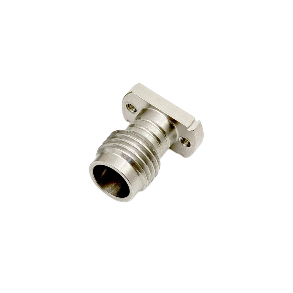
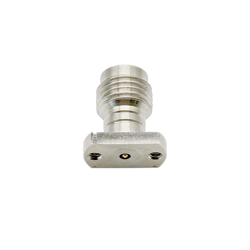
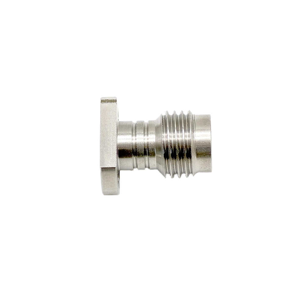
42.5 Ohm 1.85mm Jack Solderless PCB Connector DC–67 GHz VST-CPM185F-06
P/N: VST-CPM185F-06
- For 85 ohm differential launch structures
- Low-impedance design for reduced reflection
- Solderless format for repeatable board-side installation
- Well suited to high-speed data and semiconductor test
- Supports mmWave applications through 67 GHz
Engineering Note:
The VST-CPM185F-06 is a high-precision 42.5 Ω low-impedance connector engineered to suppress signal reflection in impedance-sensitive systems and is specifically matched for 85 Ω differential environments. It delivers superior phase linearity across the full DC-67 GHz spectrum, ensuring signal integrity in mission-critical millimeter-wave architectures where traditional 50 Ω components may cause mismatch.
Technical Specifications
| Impedance | 42.5 ± 1 Ω |
|---|---|
| Frequency Range | DC ~ 67 GHz |
| VSWR | ≤ 1.35 |
| Material (Body) | Stainless Steel (Passivated) |
| Material (Contact) | Beryllium Copper (Gold Plated) |
| Dielectric | High-Stability PEI |
| Insulation Resistance | 5000 MΩ |
Target Applications
AI Server & High-Speed Data
Optimized for 85 Ω differential impedance systems. Ideal for testing AI server backplanes where 42.5 Ω single-ended matching is critical for signal integrity.
6G & mmWave Research
Supports ultra-high frequencies up to 67 GHz, providing a stable interface for next-generation telecommunications and radar verification.
Semiconductor Characterization
Solderless compression design enables high-speed RF testing on evaluation boards without the thermal damage or parasitics associated with soldering.
Engineering Support
Need a Quote or Technical Support?
Share the part number, required quantity and application requirements. Our engineering team can assist with product selection, configuration review and quotation support.
Product selection support
Custom configurations available
Specification and compatibility review


-500x500.jpg)